
Concept explainers
Videos
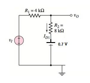
Each diode cut−in voltage in the circuit in Figure P2.59 is 0.7 V. Determine
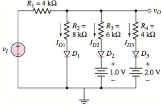
Figure P2.59
(a).
The values of
Answer to Problem 2.59P
Explanation of Solution
Given Information:
The given circuit is shown below.
Calculation:
For
The input voltage is dropped across the output because the current in the circuit is zero.
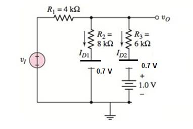
(b).
The values of
Answer to Problem 2.59P
Explanation of Solution
Given Information:
The given circuit is shown below.

Calculation:
For
The value of diode current
The modified circuit is:
Applying Kirchhoff’s voltage law:
The value of output voltage
(c).
The values of
Answer to Problem 2.59P
Explanation of Solution
Given Information:
The given circuit is shown below.

Calculation:
Assuming the diodes are in forward bias and in active mode.
Applying Kirchhoff’s current law at output node:
From above calculation diodes D1,D2 are in forward bias active mode but the diode D3 is in cut off mode because the voltage difference between positive and negative terminal is less than 0.7 V. The current through diode D3 is zero.
Hence, the assumption is incorrect.
The modified figure is:
Applying Kirchhoff’s current law at output node:
The diode currents
(d).
The values of
Answer to Problem 2.59P
Explanation of Solution
Given Information:
The given circuit is shown below.

Calculation:
For
Applying Kirchhoff’s current law at output node:
The values of diode currents are:
Want to see more full solutions like this?
Chapter 2 Solutions
Microelectronics Circuit Analysis and Design


- In the circuit, diode D1 has n = 1.4 and has an operating point I D = 1mA at V D =0.7 V and is at room temperature. Diode D2 has an area that is 20 times larger than D1 but isotherwise the same. a) What is the current through diode D1?b) What is the value of the saturation current, Is for diode D2?c) What is the voltage Vx ? d) Determine the value of R to make Vo = -0.2Varrow_forwarda. Using standard resistor values, what value of R1 is needed to achieve 1.18V ±0.01V at Vout? b. Using the R1 value chosen in (a) part, what happens to the voltage Vout when a load resistance of 10K is added (between Vout and ground). c. What is the minimum value of load resistance required for correct operation Zener diode is used in place of si diode. Or you can assume zener current according to requirement Answer it i will ratearrow_forwardFor the following circuit; a)- Diodes' conduction-cut status ("On" or "Off") determine mathematically.? (For diodes voltage drop model will be used. For each diode Vd = 0.7 V). b)- Currents passing through all branches of the circuit calculate? c)- 10 kΩ resistor on the right of the circuit Calculate the power spent on it.arrow_forward
- ⦁ Consider the below zener diode circuit and find the values of , , , . Use the constant voltage drop model which is shown is Figure 2. Show your solution steps clearly and explain them. The answers without solution steps will not be graded. Also, state your results in the sections below the circuits. ( = 0.1 )arrow_forwarddiode zener a, DESIGN THE NETWORK IN THE FIGURE, TO KEEP, "VL" at 12 V for a variation in load (IL) from 0 to 200 mA, DETERMINE "Rs" and "Vz" b. determine "P2min" for the Zener diode from section aarrow_forwardIn the circuit shown in Figure 2–52 (p. 97), the Zener diode has a reverse breakdown voltage of 12V. RS = 50 Ohms, VS = 20V, and RL can vary from 100 Ohms to 200 Ohms. Assuming that the Zener diode remains in breakdown, find: (a) the minimum and maximum current in the Zener diode; (b) the minimum and maximum power dissipated in the diode; and (c) the minimum rated power dissipation that RS should have.arrow_forward
- 2.13 Two diodes are connected in series as shown in Figure 2.11a to share a total de reverse volt age of VD=5 KV. The reverse leakage currents of two diode I=25 mA, 1,2 = 30 mA. (a) Find the diode voltage if the voltage sharing resistances R₁ and R₂ are equal R₁ = R₂ = 200 KN. (b) Find the voltage sharing resistance R₁ and R₂ if the diode voltage are equal Vd1= Vd2= Vd/2arrow_forwardHow are diodes tested for functionality? Write the necessary devices/materials needed to do the test and discuss thoroughly the procedure.arrow_forwardIn a 1-phase full wave bridge rectifier with Vs = Vm sin ωt, with R load & ideal diodes. The expression for the average value of the output voltage is 2Vm/π Select one: True Falsearrow_forward
- The carrier concentrations (Figure 1) are approximations for the case where the net (n-type or p-type) doping of the semiconductor is very well defined (>> ni ). For generic semiconductor doping, the relations in Figure 2 take effect. Deduce the relations from Figure 2.arrow_forwardThe applied electric field in p-type silicon is E=10V/cm. The semiconductor conductivity is 1.5(Ω-cm)-1and cross-sectional area is 10-5cm2. Determine the driftcurrent. (b) A drift current density of 120A/cm2is established in n-type silicon with an applied electric field of 18V/cm. If the electron and hole mobilities are µn =1250 cm2/V-s and µp =450 cm2/V-s, respectively, determine the required doping concentration.arrow_forwardCalculate the V0 voltage and the ID1 current in the circuit given with figure 2, If R1=10kohm, R2=5kohm and forward diode voltage is 0.7V ..arrow_forward
