Concept explainers
Videos
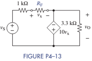
In the circuit of Figure P4-13, the VCVS has of 10,
Want to see the full answer?
Check out a sample textbook solution
Chapter 4 Solutions
EBK THE ANALYSIS AND DESIGN OF LINEAR C


- Figure Q4(b) shows an amplifier block diagram. Design using MORE THAN ONE op-amps which have one common input signal and two output signals. Shows all necessary calculation of the design. Vil: - 200mV Figure Q4(b) • Vo2 = 20mV Vo3 = - 1Varrow_forwardR, V OUT Let currents and node voltage for the Op-Amp circuit be defined as follows: |1 equals the current flowing through Rin from left to right. Let Vb be the voltage at the inverting input (-). Write 1 in terms of the node voltages Vin, Vb (voltage at inverting input). O Vb - Vin O Vvin - Vb O (Vb - Vin)/Rin O Vin - Vb) / Rin O - Vin/Rinarrow_forwarddesign op-amp circut to give the following output v=2v1-3v2+12v3-6v4arrow_forward
- A real opamp in a closed loop circuit is operating in saturation mode. The output voltage is not increasing despite increases in the input. The supply voltages are -15V and +15V. Identify all the true statements below. The max output voltage will be around 13 V. O The max output voltage will be around 30 V. O The Opamp inverting and non-inverting inputs may no longer be equal. O The current into the OpAmp may increase. O The output voltage will eventually go to zero. O The input voltages will be virtual grounds.arrow_forwardSolve for V2 given the value of V0 and assuming the opamp is idealarrow_forwardDesign an op-amp circuit to yield the relationship shown in each equation. Vo = V1 + 10V2 – 30V3 – 100 V4a.) Rmin = 6kΩb.) Rin = 6kΩarrow_forward
- Av=50 of the voltage gain according to the circuit in Figure what should be the value of resistance R4 to be. [R3 = 0.5 kΩ]arrow_forwardVz=6.3V , open loop voltage gain AoL = Vol/Vd = 1000, (Vd= V+ - V-), output current Io is , when there is no load 1mA, when there is full load 100mA. What is the load regulation?arrow_forwardQ4: Baginning in position1 in figure,the switch is thrown into position2 and held there for 10ms, then back to position1 for 10ms,and so forth.sketch the resulting output waveform if its initial value is 0v, the saturated output levels of the op-amp +-12v? +5V R. 10LF 10K2 -5Varrow_forward
- Design op-amp ciran't produce Even odd to each of following outputs. -026=0-42₂ - 10%, @v₂ = 84 — 32/₂₁ +423-924 (2) V = V₁ + V₂ - 2013 @ 2 = 252₁ +32 Vaarrow_forward10 kN and R 30 kn. Assume that the op- 4-23. Consider the circuit of Figure P4-11 with R¡ amp slew rate is 0.5 V/us. Calculate the rise time TSR due to the slew rate when the input is a pulse that changes from zero to each of the following values: a. 0.2 V b. 1 V c. 3 V SR = type your answer... a) Tsr = b) Tsr= c) Tsr = type your answer... type your answer... type your answer... FIGURE P4-11 R₁ ww + Rfiq ww + Voarrow_forward2. What op-amp configuration is this circuit? Fill in the value for this circuit to have an Av=5.7. RI= 1k ohm. RI www Vin RF U1 Vout W RI = RF =arrow_forward
 Introductory Circuit Analysis (13th Edition)Electrical EngineeringISBN:9780133923605Author:Robert L. BoylestadPublisher:PEARSON
 Delmar's Standard Textbook Of ElectricityElectrical EngineeringISBN:9781337900348Author:Stephen L. HermanPublisher:Cengage Learning
 Programmable Logic ControllersElectrical EngineeringISBN:9780073373843Author:Frank D. PetruzellaPublisher:McGraw-Hill Education
 Fundamentals of Electric CircuitsElectrical EngineeringISBN:9780078028229Author:Charles K Alexander, Matthew SadikuPublisher:McGraw-Hill Education
 Electric Circuits. (11th Edition)Electrical EngineeringISBN:9780134746968Author:James W. Nilsson, Susan RiedelPublisher:PEARSON
 Engineering ElectromagneticsElectrical EngineeringISBN:9780078028151Author:Hayt, William H. (william Hart), Jr, BUCK, John A.Publisher:Mcgraw-hill Education,