EBK THE ANALYSIS AND DESIGN OF LINEAR C
8th Edition
ISBN: 9781119140320
Author: Toussaint
Publisher: VST
expand_more
expand_more
format_list_bulleted
Concept explainers
Videos
Textbook Question
Chapter 4, Problem 4.26P
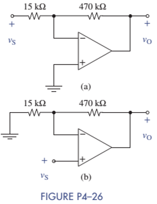
Find the voltage gain of each OP AMP circuit shown in Figure P4-26.
Expert Solution & Answer
Want to see the full answer?
Check out a sample textbook solution
Students have asked these similar questions
Q4: Find Rab for the circuit in figure below
10 kN and R 30 kn. Assume that the op-
4-23. Consider the circuit of Figure P4-11 with R¡
amp slew rate is 0.5 V/us. Calculate the rise time TSR due to the slew rate when the input is
a pulse that changes from zero to each of the following values:
a. 0.2 V
b. 1 V
c. 3 V
SR = type your answer...
a) Tsr =
b) Tsr=
c) Tsr =
type your answer...
type your answer...
type your answer...
FIGURE P4-11
R₁
ww
+
Rfiq
ww
+
Vo
I am unsure of how to find the equivalent resistance I suspect that I have to transform this into a "realistic/non-ideal" op-amp but I don't know.
Chapter 4 Solutions
EBK THE ANALYSIS AND DESIGN OF LINEAR C
Ch. 4 - Find the voltage gain vO/vS and current gain iO/ix...Ch. 4 - Prob. 4.2PCh. 4 - Prob. 4.3PCh. 4 - Prob. 4.4PCh. 4 - Find the voltage gain vO/vS in Figure P4-5.Ch. 4 - Find the voltage gain vO/vS in Figure P4-6.Ch. 4 - Find an expression for the current gain iO/iS in...Ch. 4 - Prob. 4.8PCh. 4 - Prob. 4.9PCh. 4 - Find an expression for the voltage gain vO/vs in...
Ch. 4 - Prob. 4.12PCh. 4 - In the circuit of Figure P4-13, the VCVS has of...Ch. 4 - Prob. 4.14PCh. 4 - (a) Find the Thévenin equivalent circuit that the...Ch. 4 - Prob. 4.16PCh. 4 - Prob. 4.18PCh. 4 - Prob. 4.19PCh. 4 - The circuit parameters in figure P4-21 are...Ch. 4 - The circuit parameters in Figure P4-21 are...Ch. 4 - The parameters of the transistor in Figure P4-23...Ch. 4 - Prob. 4.25PCh. 4 - Find the voltage gain of each OP AMP circuit shown...Ch. 4 - Considering simplicity and standard 10 tolerance...Ch. 4 - Two OP AMP circuits are shown in Figure P4-28....Ch. 4 - Prob. 4.29PCh. 4 - What is the range of the gain vO/vS in Figure...Ch. 4 - Using only one OP AMP, design a circuit that...Ch. 4 - Design a circuit using only one OP AMP that...Ch. 4 - Prob. 4.36PCh. 4 - For the circuit in Figure P4-37: (a) Find vO in...Ch. 4 - A young designer needed to amplify a 2-V signal by...Ch. 4 - Design two circuits to produce the following...Ch. 4 - Design a noninverting summer for five inputs with...Ch. 4 - For the circuit in Figure P4-41: Find vO in terms...Ch. 4 - The input-output relationship for a three-input...Ch. 4 - Find vo in terms of the inputs v1,v2, and v3 in...Ch. 4 - Prob. 4.44PCh. 4 - Prob. 4.45PCh. 4 - Prob. 4.46PCh. 4 - Prob. 4.47PCh. 4 - It is claimed that vO=vS when the switch is closed...Ch. 4 - Prob. 4.49PCh. 4 - Prob. 4.50PCh. 4 - Use node-voltage analysis in Figure P4-51 to show...Ch. 4 - Prob. 4.52PCh. 4 - Prob. 4.53PCh. 4 - For the block diagram of Figure P4-54: Find an...Ch. 4 - For the block diagram of Figure P4-55: Find an...Ch. 4 - For the circuit in Figure P4-56: Find vO in terms...Ch. 4 - Prob. 4.57PCh. 4 - Onan exam, students were asked to design an...Ch. 4 - Prob. 4.59PCh. 4 - For the circuit of Figure P4-60: Use node-voltage...Ch. 4 - Prob. 4.61PCh. 4 - Design a single OP AMP amplifier with a voltage...Ch. 4 - Design an OP AMP amplifier with a voltage gain of...Ch. 4 - Using a single OP AMP, design a circuit with...Ch. 4 - Design a differential amplifier with inputs v1 and...Ch. 4 - Using no more than two OP AMPs, design an OP AMP...Ch. 4 - Design a two-input noninverting summer that will...Ch. 4 - Design a three-input noninverting summer that will...Ch. 4 - Design a cascaded OP AMP circuit that will produce...Ch. 4 - Design a cascaded OP AMP circuit that will produce...Ch. 4 - Using the instrumentation amplifier shown in...Ch. 4 - Prob. 4.73PCh. 4 - Design a circuit that can produce vO=2000vTR2.6V...Ch. 4 - A requirement exists for an OP AMP circuit with...Ch. 4 - A requirement exists for an OP AMP circuit to...Ch. 4 - A particular application requires that an...Ch. 4 - Prob. 4.78PCh. 4 - The full-scale output of a six-bit DAC is 10.0 V....Ch. 4 - An R2R DAC is shown in Figure P4-80. The digital...Ch. 4 - A fifth bit is added to the R-2R DAC shown in...Ch. 4 - Prob. 4.82PCh. 4 - Prob. 4.83PCh. 4 - A small pressure transducer has the...Ch. 4 - A medical grade pressure transducer has been...Ch. 4 - The acid/alkaline balance of a fluid is measured...Ch. 4 - A photoresistor varies from 10 in bright sunlight...Ch. 4 - Your engineering firm needs an instrumentation...Ch. 4 - Prob. 4.90PCh. 4 - Prob. 4.92PCh. 4 - Prob. 4.93PCh. 4 - A five-bit flash ADC in Figure P4-94 uses a...Ch. 4 - Bipolar Power Supply Voltages The circuit in...Ch. 4 - Thermometer Design Problem There is a need to...Ch. 4 - High Bias Design Problem A particular pressure...Ch. 4 - Prob. 4.99IPCh. 4 - OP AMP Circuit Analysis and Design Find the...Ch. 4 - Instrumentation Amplifier with Alarm Strain gauges...
Knowledge Booster


Learn more about
Need a deep-dive on the concept behind this application? Look no further. Learn more about this topic, electrical-engineering and related others by exploring similar questions and additional content below.Similar questions
- Figure Q4(f) shows a 4-bit weighted resistor network DAC to convert the digital input to analog output. The internal reference, Vref = -5V. Determine the analog output for 0010, 0011, 0100, 0101, 0110, 1001, 1010 and 1100 digital input. ww Rf S3 Rn-1 D3 A VO R2 D2 RI DI RO DO V ref Figure Q4(f): 4-bit weighted resistor network DACarrow_forwardHELP a:Write the equation Vo according to the block diagram given below. b: Design the circuit that will perform the operation by using 0.5 V and 10 V direct current (DC) sources with a single OPAMP.arrow_forwardDesign Problem: Design a clamper circuit based on the input and output waveforms shown in the diagram below: Design Voltage Input Voltage Output Assign peak value of your Voltage Input and frequency. Solve theoreticallyarrow_forward
- Connect a thermistor (Resistance=500 – 1% per °C) in a bridge (power supply =8V) with an instrumentation amplifier (IA '521), and an inverting amplifier, and design so that output =4V at 30 C. Constraints: Use any value of resistors in the range 1K-100Karrow_forwardConnect a thermistor (Resistance=500 – 1% per oC ) in a bridge (power supply =AV) with an instrumentation amplifier (IÁ '521), and an inverting amplifier, and design so that output =BV at Č oC. Constraints: Use any value of resistors in the range 1K-100K A=8 , B=6 ,c=30arrow_forward3. Design an op-amp circuit (using exactly 2 op- amps) that does the following mathematical operation: 4V, + 1 3V₂ - 6V₂. 2 3°arrow_forward
- The circuit below, you may note, does not match any of the common op-amp circuits. By performing circuit analysis, determine the voltage across the load resistor R5. You may assume that V1 = 4.3 V, V2 = 5.4 V, R1 = 49 kQ, R2 = 85 KQ, R3 85 KQ, R4 = 66 kQ, and R5 = 68 kQ. = R1 V1 + R2 V2 R3 R4 R5 marrow_forwarddesign op-amp circut to give the following output v=2v1-3v2+12v3-6v4arrow_forwardGiven the circuit provided in Figure 4-30 (p. 194) and the fabrication parameters provided, find ID and VDS. VBias = 3.8V, VDD = 5V, RD= 1kΩ, RS = 1kΩ, Vt = 0.3V, kn = 100uA/V2. (NOTE: use Wolfram Alpha Equation Solver.) (b) Design a voltage divider circuit to create the bias voltage using resistors R1 and R2. Let the current through the voltage divider be in the range of 1mA to 10mA.arrow_forward
- HELP I NEED THIS QUICKLY a:Write the equation Vo according to the block diagram given below. b: Design the circuit that will perform the operation by using 0.5 V and 10 V direct current (DC) sources with a single OPAMP.arrow_forwardThe circuit below, you may note, does not match any of the common op-amp circuits. By performing circuit analysis, determine the voltage across the load resistor R5. You may assume that V1 = 5.1 V, V2 = 4.2 V, R1 = 95 kQ, R2 = 63 KQ, R3 = 40 kQ, R4 = 28 kQ, and R5 = 73 kQ. R1 V1 R2 V2 + + R3 R4 R5 mn marrow_forwardIn what application purpose that a comparator is used? ( in Non-Linear Op-Amps Applications Voltage Comparator )arrow_forward
arrow_back_ios
SEE MORE QUESTIONS
arrow_forward_ios
Recommended textbooks for you
 Introductory Circuit Analysis (13th Edition)Electrical EngineeringISBN:9780133923605Author:Robert L. BoylestadPublisher:PEARSON
 Delmar's Standard Textbook Of ElectricityElectrical EngineeringISBN:9781337900348Author:Stephen L. HermanPublisher:Cengage Learning
 Programmable Logic ControllersElectrical EngineeringISBN:9780073373843Author:Frank D. PetruzellaPublisher:McGraw-Hill Education
 Fundamentals of Electric CircuitsElectrical EngineeringISBN:9780078028229Author:Charles K Alexander, Matthew SadikuPublisher:McGraw-Hill Education
 Electric Circuits. (11th Edition)Electrical EngineeringISBN:9780134746968Author:James W. Nilsson, Susan RiedelPublisher:PEARSON
 Engineering ElectromagneticsElectrical EngineeringISBN:9780078028151Author:Hayt, William H. (william Hart), Jr, BUCK, John A.Publisher:Mcgraw-hill Education,
Introductory Circuit Analysis (13th Edition)
Electrical Engineering
ISBN:9780133923605
Author:Robert L. Boylestad
Publisher:PEARSON
Delmar's Standard Textbook Of Electricity
Electrical Engineering
ISBN:9781337900348
Author:Stephen L. Herman
Publisher:Cengage Learning
Programmable Logic Controllers
Electrical Engineering
ISBN:9780073373843
Author:Frank D. Petruzella
Publisher:McGraw-Hill Education
Fundamentals of Electric Circuits
Electrical Engineering
ISBN:9780078028229
Author:Charles K Alexander, Matthew Sadiku
Publisher:McGraw-Hill Education
Electric Circuits. (11th Edition)
Electrical Engineering
ISBN:9780134746968
Author:James W. Nilsson, Susan Riedel
Publisher:PEARSON
Engineering Electromagnetics
Electrical Engineering
ISBN:9780078028151
Author:Hayt, William H. (william Hart), Jr, BUCK, John A.
Publisher:Mcgraw-hill Education,
Why HIGH VOLTAGE DC power Transmission; Author: ElectroBOOM;https://www.youtube.com/watch?v=DFQG9kuXSxg;License: Standard Youtube License