
EBK THE ANALYSIS AND DESIGN OF LINEAR C
8th Edition
ISBN: 9781119228226
Author: Toussaint
Publisher: YUZU
expand_more
expand_more
format_list_bulleted
Concept explainers
Videos
Textbook Question
Chapter 4, Problem 4.51P
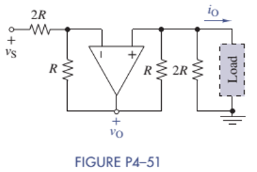
Use node-voltage analysis in Figure P4-51 to show that
Expert Solution & Answer
Want to see the full answer?
Check out a sample textbook solution
Students have asked these similar questions
determine the R4 value that results in maximum voltage magnitude across R1 for thecircuit in experiment 2. You are expected to simulate the circuit with three or more R4 values and usethe simulation results to support your answer.
p is power here find p4+p5 urgently please
Given this thevenin equivalent circuit, we now plug up a load resistor that is 500 ohms. How would you calculate output voltage and output current given this load resistor?
Chapter 4 Solutions
EBK THE ANALYSIS AND DESIGN OF LINEAR C
Ch. 4 - Find the voltage gain vO/vS and current gain iO/ix...Ch. 4 - Prob. 4.2PCh. 4 - Prob. 4.3PCh. 4 - Prob. 4.4PCh. 4 - Find the voltage gain vO/vS in Figure P4-5.Ch. 4 - Find the voltage gain vO/vS in Figure P4-6.Ch. 4 - Find an expression for the current gain iO/iS in...Ch. 4 - Prob. 4.8PCh. 4 - Prob. 4.9PCh. 4 - Find an expression for the voltage gain vO/vs in...
Ch. 4 - Prob. 4.12PCh. 4 - In the circuit of Figure P4-13, the VCVS has of...Ch. 4 - Prob. 4.14PCh. 4 - (a) Find the Thévenin equivalent circuit that the...Ch. 4 - Prob. 4.16PCh. 4 - Prob. 4.18PCh. 4 - Prob. 4.19PCh. 4 - The circuit parameters in figure P4-21 are...Ch. 4 - The circuit parameters in Figure P4-21 are...Ch. 4 - The parameters of the transistor in Figure P4-23...Ch. 4 - Prob. 4.25PCh. 4 - Find the voltage gain of each OP AMP circuit shown...Ch. 4 - Considering simplicity and standard 10 tolerance...Ch. 4 - Two OP AMP circuits are shown in Figure P4-28....Ch. 4 - Prob. 4.29PCh. 4 - What is the range of the gain vO/vS in Figure...Ch. 4 - Using only one OP AMP, design a circuit that...Ch. 4 - Design a circuit using only one OP AMP that...Ch. 4 - Prob. 4.36PCh. 4 - For the circuit in Figure P4-37: (a) Find vO in...Ch. 4 - A young designer needed to amplify a 2-V signal by...Ch. 4 - Design two circuits to produce the following...Ch. 4 - Design a noninverting summer for five inputs with...Ch. 4 - For the circuit in Figure P4-41: Find vO in terms...Ch. 4 - The input-output relationship for a three-input...Ch. 4 - Find vo in terms of the inputs v1,v2, and v3 in...Ch. 4 - Prob. 4.44PCh. 4 - Prob. 4.45PCh. 4 - Prob. 4.46PCh. 4 - Prob. 4.47PCh. 4 - It is claimed that vO=vS when the switch is closed...Ch. 4 - Prob. 4.49PCh. 4 - Prob. 4.50PCh. 4 - Use node-voltage analysis in Figure P4-51 to show...Ch. 4 - Prob. 4.52PCh. 4 - Prob. 4.53PCh. 4 - For the block diagram of Figure P4-54: Find an...Ch. 4 - For the block diagram of Figure P4-55: Find an...Ch. 4 - For the circuit in Figure P4-56: Find vO in terms...Ch. 4 - Prob. 4.57PCh. 4 - Onan exam, students were asked to design an...Ch. 4 - Prob. 4.59PCh. 4 - For the circuit of Figure P4-60: Use node-voltage...Ch. 4 - Prob. 4.61PCh. 4 - Design a single OP AMP amplifier with a voltage...Ch. 4 - Design an OP AMP amplifier with a voltage gain of...Ch. 4 - Using a single OP AMP, design a circuit with...Ch. 4 - Design a differential amplifier with inputs v1 and...Ch. 4 - Using no more than two OP AMPs, design an OP AMP...Ch. 4 - Design a two-input noninverting summer that will...Ch. 4 - Design a three-input noninverting summer that will...Ch. 4 - Design a cascaded OP AMP circuit that will produce...Ch. 4 - Design a cascaded OP AMP circuit that will produce...Ch. 4 - Using the instrumentation amplifier shown in...Ch. 4 - Prob. 4.73PCh. 4 - Design a circuit that can produce vO=2000vTR2.6V...Ch. 4 - A requirement exists for an OP AMP circuit with...Ch. 4 - A requirement exists for an OP AMP circuit to...Ch. 4 - A particular application requires that an...Ch. 4 - Prob. 4.78PCh. 4 - The full-scale output of a six-bit DAC is 10.0 V....Ch. 4 - An R2R DAC is shown in Figure P4-80. The digital...Ch. 4 - A fifth bit is added to the R-2R DAC shown in...Ch. 4 - Prob. 4.82PCh. 4 - Prob. 4.83PCh. 4 - A small pressure transducer has the...Ch. 4 - A medical grade pressure transducer has been...Ch. 4 - The acid/alkaline balance of a fluid is measured...Ch. 4 - A photoresistor varies from 10 in bright sunlight...Ch. 4 - Your engineering firm needs an instrumentation...Ch. 4 - Prob. 4.90PCh. 4 - Prob. 4.92PCh. 4 - Prob. 4.93PCh. 4 - A five-bit flash ADC in Figure P4-94 uses a...Ch. 4 - Bipolar Power Supply Voltages The circuit in...Ch. 4 - Thermometer Design Problem There is a need to...Ch. 4 - High Bias Design Problem A particular pressure...Ch. 4 - Prob. 4.99IPCh. 4 - OP AMP Circuit Analysis and Design Find the...Ch. 4 - Instrumentation Amplifier with Alarm Strain gauges...
Knowledge Booster


Learn more about
Need a deep-dive on the concept behind this application? Look no further. Learn more about this topic, electrical-engineering and related others by exploring similar questions and additional content below.Similar questions
- Q4: Suppose that the components of the circuit shown in figure below have the following values: R1-10Ω , R2-20Ω , R3-30Ω, R4-10Ω, R5-20Ω, R6-15Ω, R7- 100Ω. The voltage across AB is measured by a voltmeter whose internal resistance is 6002. What is the measurement error caused by the resistance of the measuring instrument? R5 200 RM R2 A 600 LA 12V 200 R4 R1 R7 100 1000 100 R3 R6 300 B 150arrow_forwardc) Using minimum number of components, design a voltage divider which can deliver 1 W at 100V, 2W at -50V and 1.6W at -80V. The voltage source has an internal resistance of 200 Q and supplies a current of 100mA. What is the open - circuit voltage of the voltage source? All resistance in ohm.arrow_forwardA DC voltage is added in the circuit as shown in Figure 6. Derive a new expression for the voltage gain and what can you conclude about the observation in voltage gain in response to the added DC voltage. R2 R4 R3 V. 1 V R1 Figure 6arrow_forward
- Design a Half adder, Full adder, Half Subtractor and Full Subtractor. Need the circuit diagramsarrow_forwardRead the instructions carefully and show your solutions Using a constant-voltage-drop model , design a circuit for the function shown in the figure below. VD = 0.7 V Vs vo 10 V 2.7 V Vs DESIGN vo -10 V -17.3 Varrow_forwardFind the current i for the circuit of the Figure. Hint: A short circuit can be treated as a 0-V voltage source. The value of current i in Amp isarrow_forward
- need help on Q4 ,thanksarrow_forwardVoltage Zener is used in the circuit below and the load current is to vary from 12 to 100 mA. Find the value of series resistance R and the range of load resistance to maintain a voltage of 7.2 V across the load. The input voltage is constant at 12V and the minimum Zener current is 10 mA. ... IL R Iz Eo RL Vz E, = 12 Varrow_forwardDesign the following circuit to operate as a switch, with Ic2 1. Find the value of R1, R2, R3, R4, R5 and RB. 2. Sketch the output Voltage Vo. 4.5A: v* = ! 9V V, (v) Bsat = 30 RB2 Vi Q2 R1= R2= R3= R4= R5 Q I82 9V VEB=0.7V \Ic2 -t R2 1 2 3 4 R1 R3 Vo R4 R5arrow_forward
- Develop a circuit that will provide an output voltage that is -4 Vm if the input voltage is Vmsinwtarrow_forwardConsider the P-I-N structure shown in Rg. 4-49. The I region is intrinsic. Determine the quantities in (a) and (c). Assume that no bias is applied.arrow_forwardIn the circuit shown in the figure, the variable resistance Ro is set for maximum power transfer. a) Find the Ro value b) Find the maximum power that can be transferred to Ro. Drarrow_forward
arrow_back_ios
SEE MORE QUESTIONS
arrow_forward_ios
Recommended textbooks for you
 Delmar's Standard Textbook Of ElectricityElectrical EngineeringISBN:9781337900348Author:Stephen L. HermanPublisher:Cengage Learning
Delmar's Standard Textbook Of Electricity
Electrical Engineering
ISBN:9781337900348
Author:Stephen L. Herman
Publisher:Cengage Learning
Superposition Theorem; Author: The Organic Chemistry Tutor;https://www.youtube.com/watch?v=EX52BuZxpQM;License: Standard Youtube License