
Concept explainers
Videos
For the PMOS common−source circuit shown in Figure P769, the transistor parameters are:
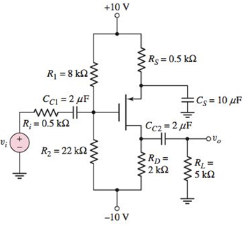
Figure P7.69
(a)
The upper
Answer to Problem 7.69P
The upper
Explanation of Solution
Given:
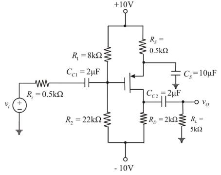
The given circuit is shown below.
Calculation:
Calculate the gate voltage
Substitute
The expression for drain current
Substitute 10 for
Consider the another expression for drain current
Equate equations (1) and (2)
Calculate source-to-gate voltage
Calculate transconductance
Substitute
Calculate the Miller Capacitance.
Substitute
Calculate the time constant
Where
Recall equation (3).
Substitute
Calculate the upper 3 dB frequency
Therefore, the upper
(b)
The value of the Miller capacitance
Answer to Problem 7.69P
The value of the Miller capacitance is
Explanation of Solution
Given:
The given circuit is shown below.

Calculation:
Calculate the gate voltage
Substitute
The expression for drain current
Substitute 10 for
Consider the another expression for drain current
Substitute
Equate equations (1) and (2)
Calculate source-to-gate voltage
Calculate transconductance
Substitute
Calculate the Miller Capacitance.
Substitute
The value of the Miller capacitance is
(c)
The mid-band voltage gain.
Answer to Problem 7.69P
The mid-band voltage gain is
Explanation of Solution
Given:
The given circuit is shown below.

Calculation:
Draw the small-signal model of the circuit shown in figure
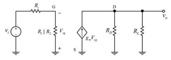
Determine the expression for output voltage
Apply the voltage division principle.
Determine source-to-gate voltage
Substitute
Substitute
Therefore, the expression for the mid-band voltage gain is,
Substitute
Want to see more full solutions like this?
Chapter 7 Solutions
MICROELECT. CIRCUIT ANALYSIS&DESIGN (LL)


- A rectangular guide with dimensions of 5.7cmX2.524cm has air as its dielectric and operates at a frequency of 4.21GHz. Get The first 4 cut-off frequencies of the TE modes and the first of the TM modes (in GHz),phase constant in TE10 mode guide (in rad / m),phase velocity in TE10 mode guide (in Mm / s),arrow_forwardIs the small signal model of the circuit correct?If yes, proceed in answering the questions; if not, correct the model first, then answer the questions. Note: ignore the parasitic capacitancesarrow_forwardTwo different (i.e. physically independent) band-limited analog message signals both having 5 kHz baseband bandwidth are given. A band-pass communication channel having a 10 kHz bandwidth (center frequency is 500 kHz) is available. Is it possible to transmit the given analog signals concurrently through this channel? If so, explain how it can be accomplished by deriving the related equations and also providing the spectrums. Also provide the transmitter and receiver structures with sufficient details.arrow_forward
- For an Armstrong indirect FM transmitter with the crystal carrier oscillating at 210 kHz, the crystal reference oscillating at 10.2 MHz, the sideband voltage is 0.018 V, the carrier input voltage to the combiner is 5V, the first and second multipliers are both 40, and the modulating signal frequency is 2 kHz, determine: a.) modulation index at the output of the combining network and the power amplifier; b.) frequency deviation at the same two points; and c.) the transmit carrier frequency.arrow_forwardUse Carson’s rule to determine the bandwidth of an FM channel when the maximum deviation allowed is 5 kHz at frequencies up to 3.333 kHz. Sketch the spectrum, showing carrier and sideband values.arrow_forward1. Select the correct statement(s) regarding amplitude modulation (AM). a. If the AM Index is greater than 1 (i.e., µAM>1), then over modulation occurs leading to signal distortion b. With AM, the message is captured as amplitude changes to the carrier’s amplitude. c. The AM modulated carrier bandwidth is dependent upon the baseband signal’s frequency bandwidth d. All of the above are correct 2. What is true about the frequency bandwidth of a modulated electrical or electromagnetic (EM) signal? a. signal bandwidth is only determined by the frequency of the unmodulated carrier wave b. modulation technique and the amount of information transmitted determines the signal’s bandwidth c. only the baseband signal determines frequency bandwidth; i.e., modulation technique has no impact on bandwidth d. a and c are true 3.Regarding carrier modulation, identify the carrier signal variable(s)…arrow_forward
- The modulating signal that is the input into an FM modulator is m(t)=2cos(10??).a) Express the time domain expression of ?(?) signal.b) Express FM signal in terms of Bessel functions.c) Sketch the frequency spectrum of the modulated signal.d) Determine the bandwidth of ?(?) occupies 98% of the total power (Carson Rule) in the acquired spectrum.e) Determine the condition of required bandwidth of ideal BPF if at least 80% of the total power appears at the output of the filter?arrow_forwardAn FM transmitter is determined to have a transmitter sensitivity of 498.716Hz/V. If the modulating signal is designed to be 15.998V, and the modulation index is kept to be at 1.5, solve for the highest upper sideband frequency in MHz considering that the carrier signal has a frequency equal to 172.255MHz.arrow_forwardA. Suppose that a modulated signal x(t) is created by taking a baseband signal and mixing it with a 250 Hz cosine signal, resulting in the passband spectrum X(f) shown below. Suppose that the modulated signal x(t) is mixed with a 200 Hz cosine signal c(t). The spectrum of the 200 Hz cosine is shown below as C(f). (Please look at the picture.) Which of the spectra above is the spectrum of the after mixing x(t) and c(t)? (Please pick among the choices in the picture) ============================================= B. Please look at the 2nd picture. Need help. Thank you.arrow_forward
- Identify how the excessive bandwidth use of FM can be overcome. (Check all that apply.) By using narrowband FM with small deviation ratios By using wideband FM with large deviation ratios By operating in the ultrahigh frequency (UHF) region By operating in the ultralow frequency (ULF) region By operating in the microwave regionarrow_forwardChose the correct answer 6- The bandwidth required for a modulated carrier depends on: a) The carrier frequency b) the signal-to-noise ratio c) the signal-plus-noise to noise ratio d) The baseband frequency rangearrow_forwardGiven the following CA configurations:A) CA_42AB) CA_4A_6BQuestions:1) Identify the CA type, duplex type, theoretical maximum bandwidth, and maximum numberof CCs for each CA configuration.2) If the CA_4A_6B has maximum bandwidth of 30 MHz, what are possible frequencyassignments for this CA configuration?arrow_forward
 Introductory Circuit Analysis (13th Edition)Electrical EngineeringISBN:9780133923605Author:Robert L. BoylestadPublisher:PEARSON
 Delmar's Standard Textbook Of ElectricityElectrical EngineeringISBN:9781337900348Author:Stephen L. HermanPublisher:Cengage Learning
 Programmable Logic ControllersElectrical EngineeringISBN:9780073373843Author:Frank D. PetruzellaPublisher:McGraw-Hill Education
 Fundamentals of Electric CircuitsElectrical EngineeringISBN:9780078028229Author:Charles K Alexander, Matthew SadikuPublisher:McGraw-Hill Education
 Electric Circuits. (11th Edition)Electrical EngineeringISBN:9780134746968Author:James W. Nilsson, Susan RiedelPublisher:PEARSON
 Engineering ElectromagneticsElectrical EngineeringISBN:9780078028151Author:Hayt, William H. (william Hart), Jr, BUCK, John A.Publisher:Mcgraw-hill Education,