
Concept explainers
(a)
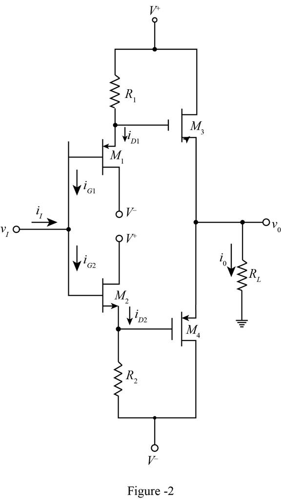
The design for class AB enhancement mode MOSFET.
(a)
Answer to Problem 8.45P
The design for class AB enhancement mode MOSFET is shown in Figure 2.
Explanation of Solution
Calculation:
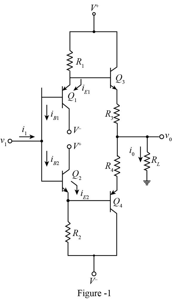
The given diagram is shown in Figure 1
The diagram for the class AB output stage using the enhancement mode MOSFETs is with resistance
The required diagram is shown in Figure 2
Conclusion:
Therefore, the design for class AB enhancement mode MOSFET is shown in Figure 2.
(b)
The value of
(b)
Answer to Problem 8.45P
The value of the resistance
Explanation of Solution
Calculation:
The expression to determine the value of the resistance
Substitute
The expression for the value of the resistance is given by,
Substitute
Conclusion:
Therefore, the value of the resistance
(c)
The value of the current in
(c)
Answer to Problem 8.45P
The value of the current
Explanation of Solution
Calculation:
The expression to determine the value of the gate to source voltage is given by,
Substitute
The expression for the gate to source voltage for
Substitute
The expression for the drain current for transitory
Substitute
The expression for the value of the drain current of transistor
Substitute
Conclusion:
Therefore, the value of the current
(c)
The current in each of the transistor, the value of the input voltage
(c)
Answer to Problem 8.45P
The value of the drain current
Explanation of Solution
Calculation:
The expression for the current through
The expression for the current through
Substitute
The conversion from
The conversion from
The expression for the value of the gate to source voltage for
Substitute
Apply KVL in at the output terminals.
Substitute
The expression for the value of the gate to source voltage for
Substitute
The expression to determine the value of the input voltage is given by,
Substitute
Apply KVL at the input terminals.
Substitute
The expression to determine the value of the drain current for
Substitute
The expression for the power delivered to the load is given by,
Substitute
Conclusion:
Therefore, the value of the drain current
Want to see more full solutions like this?
Chapter 8 Solutions
Microelectronics Circuit Analysis and Design


- For an n-channel depletion-mode MOSFET, in the saturation region ID = 8mA when VGS = 0, and the dynamic (incremental) output resistance r0 is infinite. The threshold voltage (or pinch-off voltage) is VTR = VP = –2.5V. For VGS = 0, find the smallest value of VDS at which the MOSFET is in saturation. For VDS equal to this value, find ID when (i) VGS = –1V, (ii) VGS = –2V, (iii) VGS = –3V, (iv) VGS = –4V.arrow_forwardWhat is a BJT circuit?arrow_forwardVery large-scale integration is the process of creating an integrated circuit by combining millions of MOS transistors or millions BJT transistors onto a single chip . In recent, statistics shows that electronic industries prefer MOSFET then BJT. In your own understanding could you please analyze why VLSI circuits prefer MOSFETs than BJTs?arrow_forward
- Design for an efficient 8x1 multiplexer (MUX) using CMOS technology. The primary goal is to optimize the area and power consumption while ensuring the proper functionality of the multiplexer. Utilize transmission gate technology as a part of the design process. Balance between transistor count, power efficiency, and space utilization. Note: The design should not only be functional but also efficient in terms of power and space usage, demonstrating a deep understanding of CMOS technology and multiplexer design principles.arrow_forwardIn your own understanding and words analyse why currently VLSI circuits use MOSFETs instead of BJTsarrow_forwardIn the Mosfet circuit given below, R1+R2=50 kΩ, RD= 7.5 kΩ, VDD= 5V, VTP= -0.8 V, Kp= 0.2 mA/V2 is given. Calculate the ID current by determining the working region of the mosfet.arrow_forward
- Connect the elements given below as a BJT amplifier circuit with common emitter. BJT is BC547B terminals from left to right are named collector, base and emitter respectively. 9V battery as VCC source will be used. The audio signal obtained from the microphone will be connected to the circuit as the input signal. C0 at the outlet, CI at the inlet, CE is given as a bypass capacitor.arrow_forwardfind the overall trasnfer function and range of k to make the system stablearrow_forwardGiven the Vth = 5V and the Rth = 650.3 ohms, what would the new output voltage be if you added a 500 ohm load resistor to the terminal demonstrated in the picture?arrow_forward
- A) What does VCO stand four? Show by drawing the relationship between its input and output signals. Compare VCO circuit with LC Tank circuit in terms of circuit functionality and how the output is generated in each of them. B) Compare between AM and FM in terms of noise immunity, interference, equipment complexity and cost and line of site transmission.arrow_forward2. a) Design a 9v DC oscillator circuit that produces a frequency of 500 Hz. The circuit may use a 555 timer or two transistor design(s). Show all calculations including the DC currents and bias voltages. Include the schematic and the required frequency formula(s). b) As a bonus, if a larger load were required to be connected to the chip, how would the schematic look and what components would be used to do design it? Also, as a theoretical approximation, if the 9v battery had a rating of 4 amp-hours, how long would it last powering this circuit? Show calculations to illustrate how you arrived at the answer.arrow_forwardBJT ANALYSIS. Given the figure, solve for IC and VCE.arrow_forward
 Introductory Circuit Analysis (13th Edition)Electrical EngineeringISBN:9780133923605Author:Robert L. BoylestadPublisher:PEARSON
 Delmar's Standard Textbook Of ElectricityElectrical EngineeringISBN:9781337900348Author:Stephen L. HermanPublisher:Cengage Learning
 Programmable Logic ControllersElectrical EngineeringISBN:9780073373843Author:Frank D. PetruzellaPublisher:McGraw-Hill Education
 Fundamentals of Electric CircuitsElectrical EngineeringISBN:9780078028229Author:Charles K Alexander, Matthew SadikuPublisher:McGraw-Hill Education
 Electric Circuits. (11th Edition)Electrical EngineeringISBN:9780134746968Author:James W. Nilsson, Susan RiedelPublisher:PEARSON
 Engineering ElectromagneticsElectrical EngineeringISBN:9780078028151Author:Hayt, William H. (william Hart), Jr, BUCK, John A.Publisher:Mcgraw-hill Education,