a) Why the energy band gap is also known as forbidden band gap? Sketch the energy band diagrams and the Fermi level for intrinsic, n-type and p-type semiconductor considering a bandgap of 1.2 eV, show the relative differences. b) Evaluate the situation when a silicon with region A has doping of N, = 1 x 10" cm³, region B has N, = 1 x 10 cm³ and region C has N,=1 x 10" cm²as shown in Fig. 1 (b) and sketch the depletion region of a p-i-n junction. (Please shade the depletion region clearly. Show the relative thickness of the depletion region.)
a) Why the energy band gap is also known as forbidden band gap? Sketch the energy band diagrams and the Fermi level for intrinsic, n-type and p-type semiconductor considering a bandgap of 1.2 eV, show the relative differences. b) Evaluate the situation when a silicon with region A has doping of N, = 1 x 10" cm³, region B has N, = 1 x 10 cm³ and region C has N,=1 x 10" cm²as shown in Fig. 1 (b) and sketch the depletion region of a p-i-n junction. (Please shade the depletion region clearly. Show the relative thickness of the depletion region.)

Introductory Circuit Analysis (13th Edition)
13th Edition
ISBN:9780133923605
Author:Robert L. Boylestad
Publisher:Robert L. Boylestad
Chapter1: Introduction
Section: Chapter Questions
Problem 1P: Visit your local library (at school or home) and describe the extent to which it provides literature...

Related questions
Question
Semiconductor Question*
Question 1
(please solve both questions but prioritize Q (b))
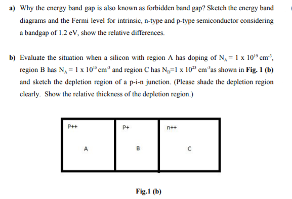
Transcribed Image Text:a) Why the energy band gap is also known as forbidden band gap? Sketch the energy band
diagrams and the Fermi level for intrinsic, n-type and p-type semiconductor considering
a bandgap of 1.2 eV, show the relative differences.
b) Evaluate the situation when a silicon with region A has doping of N, = 1 x 10® cm³,
region B has N, = 1 x 105 cm³ and region C has N,=1 x 10" cm*as shown in Fig. 1 (b)
and sketch the depletion region of a p-i-n junction. (Please shade the depletion region
clearly. Show the relative thickness of the depletion region.)
P++
P+
n++
B
Fig.1 (b)
Expert Solution
This question has been solved!
Explore an expertly crafted, step-by-step solution for a thorough understanding of key concepts.

Step by step
Solved in 3 steps with 2 images

Knowledge Booster


Learn more about
Need a deep-dive on the concept behind this application? Look no further. Learn more about this topic, electrical-engineering and related others by exploring similar questions and additional content below.Recommended textbooks for you
Introductory Circuit Analysis (13th Edition)
Electrical Engineering
ISBN:
9780133923605
Author:
Robert L. Boylestad
Publisher:
PEARSON

Delmar's Standard Textbook Of Electricity
Electrical Engineering
ISBN:
9781337900348
Author:
Stephen L. Herman
Publisher:
Cengage Learning

Programmable Logic Controllers
Electrical Engineering
ISBN:
9780073373843
Author:
Frank D. Petruzella
Publisher:
McGraw-Hill Education
Introductory Circuit Analysis (13th Edition)
Electrical Engineering
ISBN:
9780133923605
Author:
Robert L. Boylestad
Publisher:
PEARSON
Delmar's Standard Textbook Of Electricity
Electrical Engineering
ISBN:
9781337900348
Author:
Stephen L. Herman
Publisher:
Cengage Learning
Programmable Logic Controllers
Electrical Engineering
ISBN:
9780073373843
Author:
Frank D. Petruzella
Publisher:
McGraw-Hill Education

Fundamentals of Electric Circuits
Electrical Engineering
ISBN:
9780078028229
Author:
Charles K Alexander, Matthew Sadiku
Publisher:
McGraw-Hill Education

Electric Circuits. (11th Edition)
Electrical Engineering
ISBN:
9780134746968
Author:
James W. Nilsson, Susan Riedel
Publisher:
PEARSON

Engineering Electromagnetics
Electrical Engineering
ISBN:
9780078028151
Author:
Hayt, William H. (william Hart), Jr, BUCK, John A.
Publisher:
Mcgraw-hill Education,