
Videos
(a)
The value of
(a)
Answer to Problem 14.33P
The value of current
Explanation of Solution
Given:
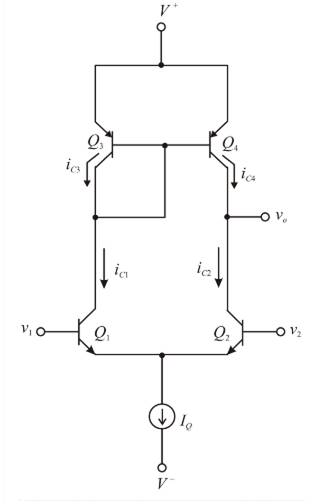
Given bipolar active load diff-amp is,

Given parameters are:
The transistor parameters are:
Calculation:
Let
Since
Now
The collector currents,
Assume that
Assume that
Taking ratio of equations (3), (5) produces,
Taking ratio of equations (4). (6) produces,
From equations (7) and (8)
Substituting equations (1) and (2) in above equation,
Given
Substituting this
(b)
The value of
(b)
Answer to Problem 14.33P
The value of current
Explanation of Solution
Given:
Given bipolar active load diff-amp is,

Given parameters are:
The transistor parameters are:
Calculation:
Let
Since
Now
The collector currents,
Assume that
Assume that
Taking ratio of equations (3), (5) produces,
Taking ratio of equations (4). (6) produces,
From equations (7) and (8)
Substituting equations (1) and (2) in above equation,
Given
Substituting this
(c)
The value of
(c)
Answer to Problem 14.33P
The value of current
Explanation of Solution
Given:
Given bipolar active load diff-amp is,
Given parameters are:
The transistor parameters are:
Calculation:
Let
Since
Now
The collector currents,
Assume that
Assume that
Taking ratio of equations (3), (5) produces,
Taking ratio of equations (4). (6) produces,
From equations (7) and (8)
Substituting equations (1) and (2) in above equation,
Given
Substituting this
Want to see more full solutions like this?
Chapter 14 Solutions
Microelectronics: Circuit Analysis and Design


- A Bipolar junction Transistor with curreat amplification factor being 100, Input Base current is 50μA. Collector voltage is 10 V and biasing voltage being +20 V. Find followings a. Collector current b. Resistance (R1) c. Collector voltage , Emitter voltage , Base Voltage & Collector-Emitter Voltage.arrow_forwardSee attached picture: Which two transistors are p-type and which two are n-type? Refer to the transistors by their labels (a, b, c, or d). Also, which transistors (a, b, c, or d) are “ON” when: A) Input A = 0, Input B = 0 B) Input A = 1, Input B = 0 C) Input A = 0, Input B = 1 D) Input A = 1, Input B = 1arrow_forwardDescribe the over-all ac analysis procedure for a common collector.arrow_forward
- In time the use of the ________ became the more desirable approach because an important parameter of the equivalent circuit was determined by the actual operating conditions rather than using a data sheet value that in some cases could be quite different. a.hybrid b.hybrid-pi c.re d.piarrow_forward6. Through the schematic symbols of MOSFETS, how can you differentiate between a depletion and an enhancement type MOSFET? P-channel or N-channel MOSFET?arrow_forwardFor the 2 circuits shown above, βnpn = 100, βpnp = 50, VDO = 0.7 V, R2 = 150 kΩ, and RB = 12 kΩ Using the ac small-scale signal analysis, determine for each circuit: a) The voltage gain (Av = vout/vin) b) The input resistance (Rin) c) The output resistance (Rout)arrow_forward
- In the circuit given in the figure, Vcc = 15V, R1 = R2 = 10k ohm, RE = 1k ohm, RL = 0.5k ohm and transistor parameters are given as VBE = 0.7V, beta (dc) = beta (0) = 100. According to this;a) Calculate the values of DC bias currents and voltages (I (BQ), I (CQ), V (CEQ)).b) Using the hybrid model of the transistor, draw the small signal equivalent circuit of the circuit.c) Derive the input impedance expression of the circuit and calculate its value.d) Derive the voltage gain expressions A (vi) and A (VG) and calculate its value.e) Derive the current gain expression A (i) = I (0) / I (i) and calculate its value. I sent you question's image. Thank you..arrow_forwardDraw the equivalent circuit for a common-emitter bipolar transistor amplifier andderive suitable formulae for the amplifier current gain, voltage gain and power gain.Neglect bias,decoupling and coupling componentsarrow_forwardWhat is the conversion gain (for n = 1) for the doubly balanced mixer as shown if IBB = 5 mA, RC = 1 kΩ, and 2 R1 = 200 Ω. What is the largest value of Vm that satsifies our small-signal assumption?arrow_forward
- Topic: Field Effect Transistor For the given circuit, determine the parameters required in each below: a. Gate Voltage (VG) b. Drain Current (ID) c. Drain-Source Voltage (VDS) d. Gate-Source Voltage (VGS) e. Source Voltage (VS) f. What biasing method was utilized in the circuit? self bias, fixed bias, voltage divider bias, or source feedback bias?arrow_forwardConstruction and analysis of common base amplifier on Uni-train hardwarearrow_forwardSketch a hierarchical TDM multiplexer system to multiplex 5 channels together. Each individual multiplexer can combine, at most 3 channels.arrow_forward
 Introductory Circuit Analysis (13th Edition)Electrical EngineeringISBN:9780133923605Author:Robert L. BoylestadPublisher:PEARSON
 Delmar's Standard Textbook Of ElectricityElectrical EngineeringISBN:9781337900348Author:Stephen L. HermanPublisher:Cengage Learning
 Programmable Logic ControllersElectrical EngineeringISBN:9780073373843Author:Frank D. PetruzellaPublisher:McGraw-Hill Education
 Fundamentals of Electric CircuitsElectrical EngineeringISBN:9780078028229Author:Charles K Alexander, Matthew SadikuPublisher:McGraw-Hill Education
 Electric Circuits. (11th Edition)Electrical EngineeringISBN:9780134746968Author:James W. Nilsson, Susan RiedelPublisher:PEARSON
 Engineering ElectromagneticsElectrical EngineeringISBN:9780078028151Author:Hayt, William H. (william Hart), Jr, BUCK, John A.Publisher:Mcgraw-hill Education,