
Videos
a.
Worst case output voltage for given circuit.
a.
Answer to Problem 14.55P
The worst case output voltage is
Explanation of Solution
Given:
The given circuit is shown below.
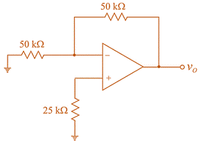
Input offset voltage
Average input bias current
Input offset current
Calculation:
On applying
For given circuit
For an op-amp
Then,
Now, KCL at input nodes:
For op-amp circuit
Now, output voltage due to input bias current and input offset current is,
Due to offset voltage,
From equation (1)
So, the worst case output voltage for the circuit will be,
b.
Worst case output voltage for given circuit.
b.
Answer to Problem 14.55P
The worst case output voltage is
Explanation of Solution
Given:
The given circuit is shown below.
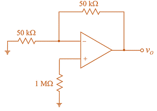
Input offset voltage
Average input bias current
Input offset current
Calculation:
Consider the circuit shwon below.
Apply KCL at non-inverting terminal
For op-amp
So,
Now, KCL at inverting terminal,
Putting
As,
And
Adding (4) and (5)
From (4)
For
For
For the circuit
If offset voltage is negative, then from (1)
Let
Putting
So, the worst case output voltage for circuit is
Want to see more full solutions like this?
Chapter 14 Solutions
Microelectronics: Circuit Analysis and Design


- Calculate the total offset voltage for the circuit shown below for op-amp specification values of input offset values, VIO=11.9 mV and IIO=62nA with RF=15 k ohm and Rin=3k ohm.arrow_forwardCalculate the total offset voltage for the circuit shown below for op-amp specification values of input offset values, VIO=2.8 mV and IIO=110 nA with RF=14000 ohm and Rin= 3000 ohm.arrow_forwardList at least five op-amp parametersarrow_forward
- Why is it that you need the higher feedback resistance (Rf) to observe saturation? (simple answer!)arrow_forwardCompare the classical Op-Amp parameters with modern Op-Amp.arrow_forward1. (a) Define analog to digital converter (ADC). Draw a 4-bit ADC circuit using Op-Amps. (b) why modulations are used in AC telemetry.Draw and discuss a basic AC data telemetry system. Please ans both parts.arrow_forward
- Problem: If the no-load output voltage of a regulator is 15.5 V and the full-load output is 14.9 V, what is the percent load regulation?arrow_forwardDiscuss the merits and demrits of feedback.arrow_forwardSketch the output voltage of the circuit shown in FigureP13.74 to scale versus time. Sometimes, an integrator circuit is used as a (approximate) pulse counter. Suppose that the output voltage is −10 V. How many input pulses have been applied (assuming that the pulses have an amplitude of 5 V and a duration of 2 ms, as shown in the figure)?arrow_forward
 Electricity for Refrigeration, Heating, and Air C...Mechanical EngineeringISBN:9781337399128Author:Russell E. SmithPublisher:Cengage Learning