
Concept explainers
Videos
A.
Worst case output voltages
A.
Answer to Problem D14.47P
Worst case output voltages are
Explanation of Solution
Given:
The given circuit is:
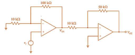
As
For first op-amp
Also
Now, KCL at input node
For second op-amp
Also
Now, KCL at input node
B.
To design:
Input bias current compensation circuit.
B.
Explanation of Solution
Given:
A simple compensation circuit can minimize the effect of bias currents in op-amp.
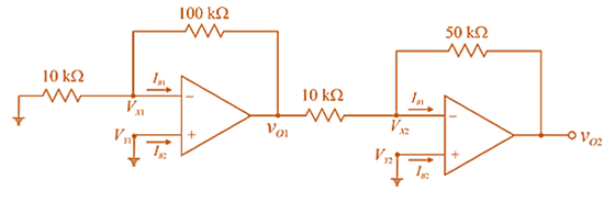
Consider the sketch ofinput bias current compensation circuit as,
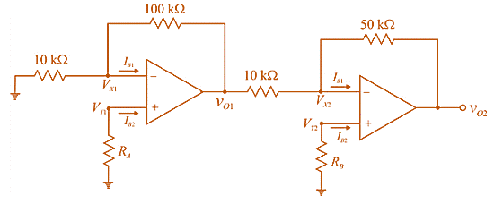
Now, determine
For first op-amp:
KCL at non-inverting node,
As,
Therefore,
KCL at inverting node,
Putting
Now,
If
For second op-amp:
KCL at non-inverting node,
As,
Therefore,
KCL at inverting node,
Putting
Now,
If
Want to see more full solutions like this?
Chapter 14 Solutions
MICROELECT. CIRCUIT ANALYSIS&DESIGN (LL)


- A resistive attenuator (e.g. coaxial cable) at room temperature has match input and output resistance and attenuation of L. Determine the equivalent temperature and noise figure of attenuator when the input source and attenuator are at room temperature. NOTE : in coaxial cable gain is 1/ attenuationarrow_forwardRouth Hurwitz analysis of closed loop system with variable gain.arrow_forwardWhy is the R-2R ladder DAC design better than a binary-weighted DAC design, particularly if you extend to 16 bits?arrow_forward
- Show 2 equations name the open loop transfer function and closed loop transfer function?arrow_forwardsubject: Communication Fundamentals Modulation and Demodulationarrow_forwardCONTROL ENGINEERING 1) Describe nontouching graph to a forward path and list down all nontouching graph(s) of the obtained Signal Flow Graph.arrow_forward
- . Explain the transducer elements with block diagram and mention the different types of displacement sensors and write the applications of LVDTarrow_forwardThe plant of a magnetic-gap controller is: Gp(s)=1/((s+f)(s-f)). A controller Gc(s)=K(s+b)(s+c)/s is proposed. Determine the gain K for marginal stability. b=0.10, c=107.00, f=62.30. Determine the gain K for Closed loop gain margin CLGM=10.7 dB. Gp & Gs are in the forward path of unity feedback system.arrow_forwardSketch the output voltage of the circuit shown in FigureP13.74 to scale versus time. Sometimes, an integrator circuit is used as a (approximate) pulse counter. Suppose that the output voltage is −10 V. How many input pulses have been applied (assuming that the pulses have an amplitude of 5 V and a duration of 2 ms, as shown in the figure)?arrow_forward
- Consider a unity feedback control system with open loop transfer function G(s) = K(s+1)/s(s+2)(s+3) The steady stare error of the system due to a unit step input is ?arrow_forwardFigure Q.4(c) shows a Schmitt Trigger circuit. Assuming that the output will saturate at ±Vsat = ±12 V and Vi = 8 sin wt [V],(i) Derive the expression for VUTP and VLTP.(ii) Draw and label the output signal, Vo.(iii) Draw and label the transfer characteristic, Vo vs Vi.arrow_forwardFor a unity feed back system, the open loop function is given by, G(s) = 90(S+9) / S2(S+2)(S+6) Determine the following: (i) The value of positional error constant is : (ii) The value of velocity error constant is : The value of acceleration error constant is : Which input signal can give correct error signal value?arrow_forward
 Introductory Circuit Analysis (13th Edition)Electrical EngineeringISBN:9780133923605Author:Robert L. BoylestadPublisher:PEARSON
 Delmar's Standard Textbook Of ElectricityElectrical EngineeringISBN:9781337900348Author:Stephen L. HermanPublisher:Cengage Learning
 Programmable Logic ControllersElectrical EngineeringISBN:9780073373843Author:Frank D. PetruzellaPublisher:McGraw-Hill Education
 Fundamentals of Electric CircuitsElectrical EngineeringISBN:9780078028229Author:Charles K Alexander, Matthew SadikuPublisher:McGraw-Hill Education
 Electric Circuits. (11th Edition)Electrical EngineeringISBN:9780134746968Author:James W. Nilsson, Susan RiedelPublisher:PEARSON
 Engineering ElectromagneticsElectrical EngineeringISBN:9780078028151Author:Hayt, William H. (william Hart), Jr, BUCK, John A.Publisher:Mcgraw-hill Education,