
Concept explainers
Videos
The loop gain, the frequency of the oscillation and the required ratio of the resistance to obtain the oscillation for the given function.
Answer to Problem 15.40P
Explanation of Solution
Given:
The circuit is given as:
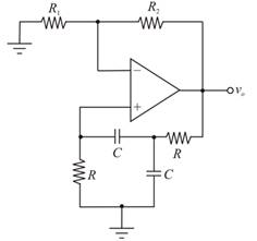
For the ideal operation amplifier, the inverting and non-inverting terminal currents should be 0. The inverting and non inverting node voltages should be equal by the virtual ground concept.
Redrawing the above circuit:
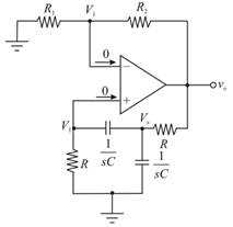
Applying Kirchhoff s current law at node
Hence,
Applying Kirchhoff s current law at non-inverting node:
Substituting
Therefore, the feed-back gain is given as:
Applying Kirchhoff s current law at inverting node:
Therefore,
The loop gain is known as the multiplication of the amplifier gain and the feedback transfer function gain as shown below:
Therefore,
The transfer function is
Put
Therefore,
For frequency oscillation the real part should be 0:
Therefore,
The frequency oscillation is
For the oscillation, the imaginary part is equal to 1:
Therefore,
Want to see more full solutions like this?
Chapter 15 Solutions
MICROELECT. CIRCUIT ANALYSIS&DESIGN (LL)


- Short answer please. What are the main disadvantages of designing the band reject filter, mentioned above? Suggest a butter circuit design.arrow_forwardDefine the following terms for FSK modulation: frequency deviation, modulation index, and deviation ratio.arrow_forwardHow to tell the difference between a open loop transfer function and closed loop transfer function?arrow_forward
- Introduction of active band pass filter ?arrow_forwardWhat is the purpose of the amplitude limiter to FM Demodulation?arrow_forwardDiscuss the ff. topics in outline form 1.Methods of generating SSB (include the block diagram) Filter method Phase shift method Weaver method 2. Block diagram and difference of Low level modulation and high level modulation 3. Low level modulator: circuit diagram and operation Diode modulator Transistor modulator 4. High level modulator: circuit diagram and operation Collector modulatorarrow_forward
- Figure Q.4(c) shows a Schmitt Trigger circuit. Assuming that the output will saturate at ±Vsat = ±12 V and Vi = 8 sin wt [V],(i) Derive the expression for VUTP and VLTP.(ii) Draw and label the output signal, Vo.(iii) Draw and label the transfer characteristic, Vo vs Vi.arrow_forwardDescribe the importance of using Bandpass filters in BFSK noncoherent demodulator.arrow_forwardwhat is the magnitude gain of Low pass butterworth filter., 6th order.arrow_forward
- calculate the loop gain voltage for the circuit shown in this image given that the unity gain frequency of the LF157A is 20MHZ and output for 1kHz and 10 MHz.arrow_forward(a) Explain any two factors which justify the need of modulating a low frequency signal. (b) Write two advantages of frequency modulation over amplitude modulation.arrow_forwardQ) What is the need of amplitude modulation?arrow_forward
 Introductory Circuit Analysis (13th Edition)Electrical EngineeringISBN:9780133923605Author:Robert L. BoylestadPublisher:PEARSON
 Delmar's Standard Textbook Of ElectricityElectrical EngineeringISBN:9781337900348Author:Stephen L. HermanPublisher:Cengage Learning
 Programmable Logic ControllersElectrical EngineeringISBN:9780073373843Author:Frank D. PetruzellaPublisher:McGraw-Hill Education
 Fundamentals of Electric CircuitsElectrical EngineeringISBN:9780078028229Author:Charles K Alexander, Matthew SadikuPublisher:McGraw-Hill Education
 Electric Circuits. (11th Edition)Electrical EngineeringISBN:9780134746968Author:James W. Nilsson, Susan RiedelPublisher:PEARSON
 Engineering ElectromagneticsElectrical EngineeringISBN:9780078028151Author:Hayt, William H. (william Hart), Jr, BUCK, John A.Publisher:Mcgraw-hill Education,