Concept explainers
Videos
Using the y parameters, derive formulas for Zin, Zout, Ai, and Av for the common-emitter transistor circuit.
Derive the formulae for input impedance, output impedance, current gain, and voltage gain for the common-emitter transistor circuit using y parameters.
Explanation of Solution
Formula used:
Write the expressions for admittance parameters of a two-port network as follows:
Refer to Figure 19.56 (a) for schematic circuit of common-emitter amplifier (transistor) and write the formulae for input impedance, output impedance, current gain, and voltage gain for the common-emitter transistor circuit as follows:
Write the expression for voltage gain of a common-emitter transistor as follows:
Here,
Write the expression for current gain of a common-emitter transistor as follows:
Here,
Write the expression for input impedance of a common-emitter transistor follows:
Write the expression for output impedance of a common-emitter transistor as follows:
Calculation:
Draw a two-port circuit to obtain input impedance, current gain, and voltage gain for the common-emitter transistor circuit as shown in Figure 1.
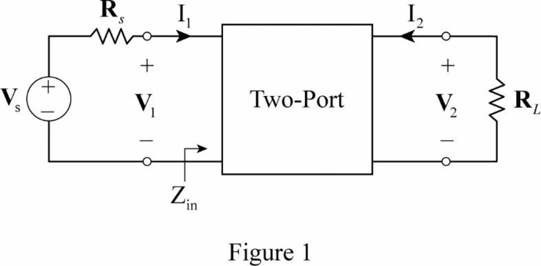
From Figure 1, write the expression for current
Substitute
Substitute
Consider
As the
Rearrange the expression as follows:
Substitute
As the current
Modify the expression in Equation (7) for common-emitter transistor circuit as follows:
Substitute
Substitute
From Equation (8), substitute
Substitute
Draw a two-port circuit to obtain output impedance for the common-emitter transistor circuit as shown in Figure 2.
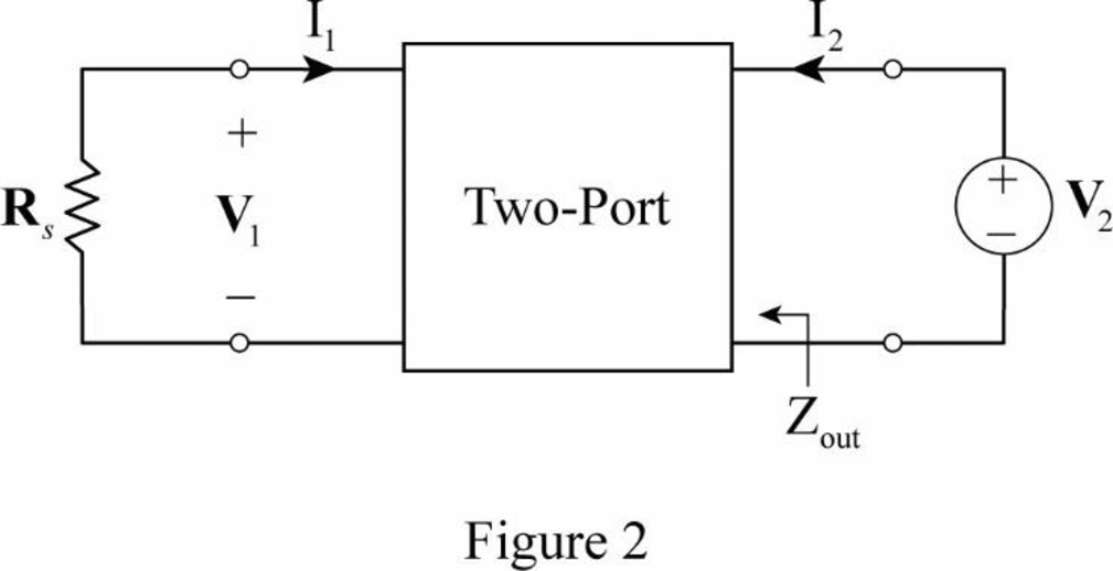
From Figure 2, write the expression for output impedance as follows:
From Equation (2), substitute
From Figure 2, write the expression for
Substitute
Substitute
From the calculations, the formulae for input impedance, output impedance, current gain, and voltage gain for the common-emitter transistor circuit are derived as follows:
Conclusion:
Thus, the formulae for input impedance, output impedance, current gain, and voltage gain for the common-emitter transistor circuit are derived.
Want to see more full solutions like this?
Chapter 19 Solutions
EBK FUNDAMENTALS OF ELECTRIC CIRCUITS


- Simplify the following functions, and implement them with two-level NAND gate circuits:arrow_forward6. Find the truth table for the circuit shown. Determine the ON/OFF condition of each transistor for all inputs. Explain your solution, briefly. A O Rb1 20k 01 Rb2 20k +5 V 02 RC 47k -OCarrow_forwardQ. No.4 Simplify the following functions, and implement them with two-level NAND gate circuits: F (W.XY.Z) =E (1,6,7,12,13,14,15)arrow_forward
- QUESTION 3 Which of the following are TRUE when the NPN transistor is saturated? a. VCE = 0.2 V b.VBE = 0.7 V C. IE = IC + IB d.IC> 0 and IB > 0arrow_forward2. From physical analysis why Is is far smaller than Ic ? 3. How must the two transistor junctions be biased for proper transistor amplifierarrow_forwardThe parameters of the transistor below are VTN = 0.6 V and Ka = 0.5 mA/V?, find the value of R1, R2, Rp such that IpDQ = 0.5689 mA, VDSQ = 1 V and R1+R=90 k2. Sketch the load line and plot the Q-point. v*= +2.5 V Rp R R2 V---2.5 V wwarrow_forward
- The following measurements are made in a two-port resistor circuit. According to this: a) Find the Z parameter matrix of the two-port circuit. b) How many volts will the open circuit voltage of gate-2 be when 80V is applied from gate-1? Calculate.arrow_forward人工知能を使用せず、 すべてを段階的にデジタル形式で解決してください。 ありがとう SOLVE STEP BY STEP IN DIGITAL FORMAT DON'T USE CHATGPT Problem 3. Calculate the mathematical expression to calculate the resistance R, given the reference current Iref and the base-emitter voltages of the transistors as well as the bias voltages known. 2 WREF 2 Vcc OK -VEE OsK Figure 3. Current controller with BJT.arrow_forwardPleasearrow_forward
- FET Construction 1. In the depletion type MOSFET there are two modes of operation : 1 2 2. In an n-channel enhancement type MOSFET if VGS = OV and VDS > Ov then ID >0 A. a) True. b) False. (if false correct the answer) 3. When a negative potential is applied to the gate terminal of a depletion type MOSFET transistor, the number of free carriers at the channel are 4. In an n-channel depletion type MOSFET consider the situation if VGS is kept constant and Vos is increased. Explain briefly what will happen to the channel if Vos is increased further. 5. In an n-channel enhancement type MOSFET if VDs ≥ VGS - Vth and VGS Vth then Ip 6. In an enhancement type MOSFET if: a) VGs > Vth and Vos = Ov then the shape of the channel is b) VGS > Vth and VDs > Ov then the shape of the channel is 7. In an n-channel depletion type MOSFET V, is a p-channel depletion type MOSFET V₁ is while forarrow_forwardSimplify the following functions, and implement them with two-level NAND gate circuits: F (W,X,Y,Z) = Ʃ (1,6,7,12,13,14,15)arrow_forwardA certain transistor has β = 50, IES = 10^(-14) A, ??? = 5 V, and ?? = 10 mA.Assume that VT = 0.026 V. Find ???, ???, ??, ??, and ?.arrow_forward
 Introductory Circuit Analysis (13th Edition)Electrical EngineeringISBN:9780133923605Author:Robert L. BoylestadPublisher:PEARSON
 Delmar's Standard Textbook Of ElectricityElectrical EngineeringISBN:9781337900348Author:Stephen L. HermanPublisher:Cengage Learning
 Programmable Logic ControllersElectrical EngineeringISBN:9780073373843Author:Frank D. PetruzellaPublisher:McGraw-Hill Education
 Fundamentals of Electric CircuitsElectrical EngineeringISBN:9780078028229Author:Charles K Alexander, Matthew SadikuPublisher:McGraw-Hill Education
 Electric Circuits. (11th Edition)Electrical EngineeringISBN:9780134746968Author:James W. Nilsson, Susan RiedelPublisher:PEARSON
 Engineering ElectromagneticsElectrical EngineeringISBN:9780078028151Author:Hayt, William H. (william Hart), Jr, BUCK, John A.Publisher:Mcgraw-hill Education,