Calculate the voltage gain, current gain, input impedance, and output impedance for the transistor network shown in Figure 19.132 in the textbook.
Answer to Problem 93P
The voltage gain, current gain, input impedance, and output impedance for the transistor network are
Explanation of Solution
Given Data:
Refer to Figure 19.132 in the textbook for the transistor network circuit.
From the given transistor network circuit, the internal resistance
Formula used:
Refer to Equation 19.73 in the textbook and write the expression for voltage gain of a transistor network in terms of hybrid parameters as follows:
Here,
Write the expression for current gain of the transistor network as follows:
Here,
Write the expression for input impedance of the transistor network as follows:
Calculation:
Redraw the given circuit as shown in Figure 1.
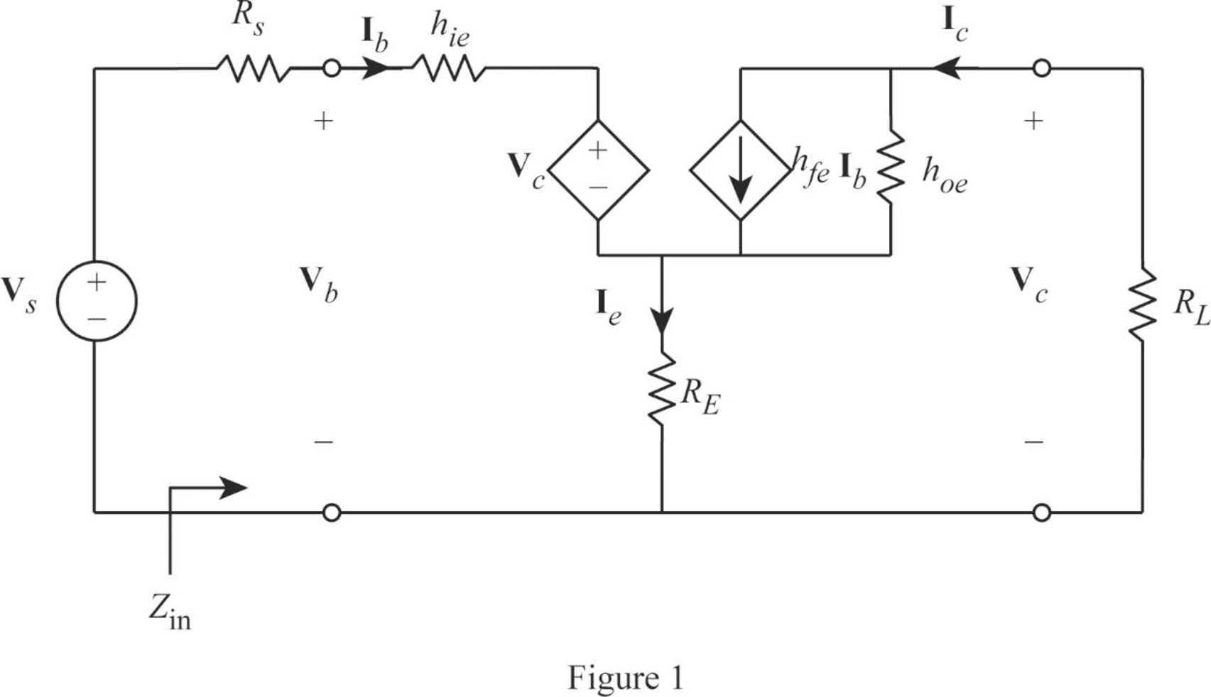
From Figure 1, write the expression for emitter current as follows:
Write the expression for base voltage from the circuit in Figure 1 as follows:
Write the expression for collector current as follows:
Write the expression for collector voltage as follows:
From Equation (7), substitute
Rearrange the expression as follows:
From Equation (2), substitute
Substitute 150 for
From Equation (6), substitute
Rearrange the expression as follows:
Rearrange the expression in Equation (5) as follows:
From Equations (7) and (9), substitute
Rearrange the expression as follows:
Substitute 150 for
Simplify the expression as follows:
From Equation (1), substitute
From Equation (9), substitute
Rearrange the expression as follows:
Substitute 150 for
From Equation (3), substitute
Consider output voltage
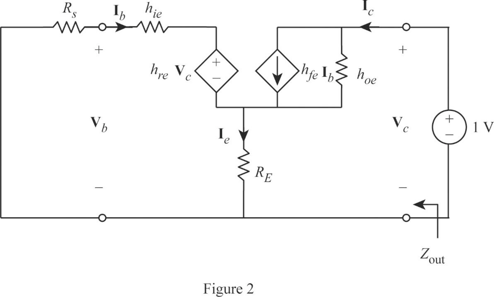
Apply KVL to the input loop for the circuit in Figure 2 as follows:
Substitute 1 for
Apply KCL at the output node for the circuit in Figure 2 as follows:
Substitute 1 for
Rearrange the expression as follows:
From Equation (12), substitute
Substitute 150 for
Write the expression for output impedance of the transistor network as follows:
Substitute 1 for
Conclusion:
Thus, the voltage gain, current gain, input impedance, and output impedance for the transistor network are
Want to see more full solutions like this?
Chapter 19 Solutions
EBK FUNDAMENTALS OF ELECTRIC CIRCUITS

- Electrical Engineering 18. For the given circuit which one of the following is the correct state equation : 0.5H +0.25F 10 320 v 10 O (b) (c) (d)arrow_forwardSketch ir and vo for the network below for the input shown. 10 k2 10 V Si 5.3 V 7.3 V - -10 Varrow_forward2. Find the hybrid parameters of the following circuit. 1 F V1 1 FZ 1 Ω 1 F 201 1Ω· 02arrow_forward
- (1I) Determine the magnitudes and directions of the currents through R, and R, in Fig. 19 R1 R2 59. V=9.0 V R=220 R2= 18 2 V3=6.0 V FIGURE 19-59arrow_forward2. (a) Overlay error is checked at the top, bottom, left and right edges, and center of a 4-inch Si wafer. The observed errors in x and y (in um) are found to be: um T. L. B 0.3 0.0 0.0 0.7 0.5 1.0 y 0.7 1.0 0.5 0.3 Analyze the error in/out, rotational and translational misalignment (b) Discuss the advantage and disadvantage of a projection lithography process.arrow_forwardFor the common-base network, determine the following: (a) Rc (b) IB (c) IE (d) VBC (e) VCE 14 V Vc=8V 4 Vo Rc RE H V₂ B=90 HoVi HH *1.1 ΚΩarrow_forward
- A Cúk converter input voltage is 200V and output of 50V, the switching frequency is 10kHz, the input and output inductances L1 and L2 value is 200puH and input and output capacitors C1 and C2 are 500µF. Load resistance is 50. The average value of the input inductor (L1) voltage is: İLi, + ¢L C, ia L2 "a本 va Load V V, Vam VT Go Soloct ono:arrow_forwardFind the hybrid integers in a two-port network. (e-1 (rad/sec)) mm 04H V₁ à ₁ (2) 211 ₁24 AM 18 12 2.5F HH I V₂arrow_forwardA transistor is used as a switch and the waveforms are shown below. The parameters are given as follows: Vcc = 150 V, VBE(sat) = 5 V, Igs = 10 A, VCE(sat) = 2 V, Ics = 120 A, ta = 0.5 us, t, = 1 us, ts = 2 us, tf = 2 us and f =10 KHz, k = 50 % and ICEO = 1 mA. The conduction time t, and the blocking time t, are equal to: VCE Vcc VCE(s31) ton toff Ics ICEO ig Select one: O a. 46 µs, 48 us O b. 20 us, 45 µs O C. 48.5 us, 46 µs o d. 45 µs, 20 µsarrow_forward
- 3. Determine i(t) in the circuit below for t20. 0.2 V 0.1 Ω mn 0.2 H m iL t=0/ 0.1 V 0.3 Ω www 0.2 Farrow_forwardThe voltage in a circuit is determined at various times, as follows: time: 123 45 67 89 voltage: 1.3 2.3 3.3 4.1 4.4 5.4 6.1 7.2 8.0 1- Fit a curve of order 3 through the data points 2- Plot this line along with the sample voltages, the sample points with red circuils and the curve with black color 3- According to your curve, determine at what time the voltage would be 2.5 V.arrow_forwardThe Si transistor has negligible leakage current and ß= 100. If Vc= 15V, V= 4V, R;= 3.3k2 and R=7.1k2. Find lag and Vaa 61+ Vcc - VEE 1O R. Rc Cc + Ccarrow_forward
 Introductory Circuit Analysis (13th Edition)Electrical EngineeringISBN:9780133923605Author:Robert L. BoylestadPublisher:PEARSON
 Delmar's Standard Textbook Of ElectricityElectrical EngineeringISBN:9781337900348Author:Stephen L. HermanPublisher:Cengage Learning
 Programmable Logic ControllersElectrical EngineeringISBN:9780073373843Author:Frank D. PetruzellaPublisher:McGraw-Hill Education
 Fundamentals of Electric CircuitsElectrical EngineeringISBN:9780078028229Author:Charles K Alexander, Matthew SadikuPublisher:McGraw-Hill Education
 Electric Circuits. (11th Edition)Electrical EngineeringISBN:9780134746968Author:James W. Nilsson, Susan RiedelPublisher:PEARSON
 Engineering ElectromagneticsElectrical EngineeringISBN:9780078028151Author:Hayt, William H. (william Hart), Jr, BUCK, John A.Publisher:Mcgraw-hill Education,