Concept explainers
Videos
Find the voltage gain
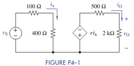
Voltage gain
Answer to Problem 4.1P
The values are
Explanation of Solution
Given:
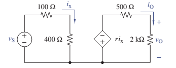
Calculation:
Apply KVL to the first loop,
Apply KVL to the second loop,
But
Divide equation (2) by equation (1).
Want to see more full solutions like this?
Chapter 4 Solutions
ANALYSIS+DESIGN OF LINEAR CIRCUITS(LL)
Additional Engineering Textbook Solutions
Electric Circuits (10th Edition)
Basic Engineering Circuit Analysis
Fundamentals of Applied Electromagnetics (7th Edition)
Introductory Circuit Analysis (13th Edition)
Electrical Engineering: Principles & Applications (7th Edition)
Electric Circuits. (11th Edition)


- these Questions from ELECTRONICS LAB ,The name of Experement is Op-Amp Inverting and Noninverting Amplifiers.arrow_forwardCan someone explain this problem step by step please. Any help will be appreciatedarrow_forward4. Calculate the output voltage of each of the following op-amp circuit. X1 Hop thi -1.5V Y11V R3 1kQ VCC 15.0V VEE -15.0V U1 -741 VCC 15.0V VEE -15.0V R4 2kQ 741 U2 R1 22.210. R2 • 1 ΚΩ ww/li R5 ww 1kQ R6 1kQ VCC 15:0V VEE -15.0V R7 1k0 U3 741 VOUTarrow_forward
- is known that all the input voltages of the circuit are equal to 12 V with the resistance R3 = R4 = R5, and Rf = 12kOhm. If you want an output voltage of -4/3 of the input voltage, then how much magnitudeof R1 and R2 if R1 = ½ (R2)?arrow_forwardshow steps pleasearrow_forwardFind parameters...arrow_forward
- V Dp Figure 1 V DD d|M2 M6 CLK –d|M4 CLK - |Mg D CLK –|M3 CLK –|M7 QM M1 M5 Master Stage Slave Stagearrow_forwardIf you need, use multisim. If you have a graphic drawing, it is preferred to draw legibly on paper. thanksarrow_forwardDetermine the regulated output voltage of the circuit in Figure D IN4O02 Vour LM317 R 2402 D2 ADI IN4002 120 V ms 470uF 1.8 kQ 000arrow_forward
- A specific p-channel JFET has a VGS(OFF) = +6 V. What is the ID when VGS= +8 V? a. VGS O b.6 V O c. VCC O d. Zeroarrow_forward4.A. Draw the expected output voltage waveform of the following circuits: |+ + VDI -| D₁ + a Vp VS - ++ R w ŵ D₂ D+ Vo |+ VD2 | io +arrow_forwardVoltage Zener is used in the circuit below and the load current is to vary from 12 to 100 mA. Find the value of series resistance R and the range of load resistance to maintain a voltage of 7.2 V across the load. The input voltage is constant at 12V and the minimum Zener current is 10 mA. ... IL R Iz Eo RL Vz E, = 12 Varrow_forward
 Introductory Circuit Analysis (13th Edition)Electrical EngineeringISBN:9780133923605Author:Robert L. BoylestadPublisher:PEARSON
 Delmar's Standard Textbook Of ElectricityElectrical EngineeringISBN:9781337900348Author:Stephen L. HermanPublisher:Cengage Learning
 Programmable Logic ControllersElectrical EngineeringISBN:9780073373843Author:Frank D. PetruzellaPublisher:McGraw-Hill Education
 Fundamentals of Electric CircuitsElectrical EngineeringISBN:9780078028229Author:Charles K Alexander, Matthew SadikuPublisher:McGraw-Hill Education
 Electric Circuits. (11th Edition)Electrical EngineeringISBN:9780134746968Author:James W. Nilsson, Susan RiedelPublisher:PEARSON
 Engineering ElectromagneticsElectrical EngineeringISBN:9780078028151Author:Hayt, William H. (william Hart), Jr, BUCK, John A.Publisher:Mcgraw-hill Education,