Microelectronics Circuit Analysis and Design
4th Edition
ISBN: 9780077387815
Author: NEAMEN
Publisher: DGTL BNCOM
bartleby

Videos

Textbook Question
Book Icon
Chapter 5, Problem D5.89DP

The emitter−follower circuit shown in Figure P5.89 is biased at
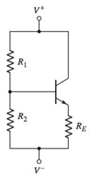
 V + = 2.5 V and V = 2.5 V . Design a bias−stable circuit such that the nominal Q−point values are I C Q 5mA and V C E Q 2.5 V . The transistor current gain values are in the range 100 β 160 . Select standard 5 percent tolerance resistance values in the final design. What is the range in Q−point values?

Chapter 5, Problem D5.89DP, The emitterfollower circuit shown in Figure P5.89 is biased at V+=2.5V and V=2.5V . Design a
Figure P5.89

Expert Solution & Answer
Check Mark
To determine

The design parameters of the circuit.

To select: Five percent tolerance values of resistances.

To find: The range of the Q- point values.

Answer to Problem D5.89DP

The design parameters of the circuit are:

  R1=8.65kΩ , R2=19.61kΩ it is closest to 19.61kΩ and RE=0.5kΩ .

Five percent tolerance resistance R1=8.2kΩ and is closest to 8.65kΩ , R2=20kΩ it is closest to 19.61kΩ and RE=0.51kΩ it is closest to 0.5kΩ .

The range of the current is 4.963mAICQ3.236mA , range of the voltage is 2.47VVCEQ3.35V .

Explanation of Solution

Given:

The given circuit is shown in Figure 1
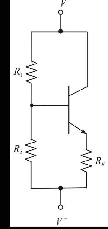
  Microelectronics Circuit Analysis and Design, Chapter 5, Problem D5.89DP , additional homework tip  1

Figure 1

Calculation:

Mark the current as well as other parameters and then redraw the circuit.

The required diagram is shown in Figure 2
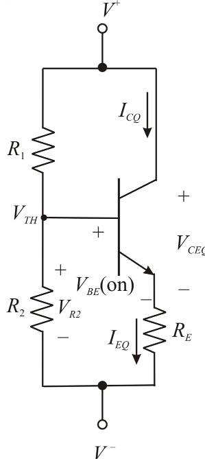
  Microelectronics Circuit Analysis and Design, Chapter 5, Problem D5.89DP , additional homework tip  2

Figure 2

The Thevenin equivalent bias circuit is shown in Figure 3
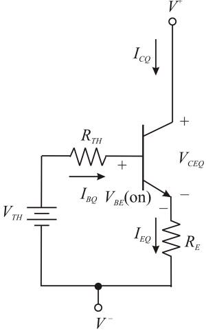
  Microelectronics Circuit Analysis and Design, Chapter 5, Problem D5.89DP , additional homework tip  3

Figure 3

The value of the base current is calculated as,

  IBQ=ICQβ

Substitute 5mA for ICQ and 120 for β in the above equation.

  IBQ=5mA120=41.67μA

Apply KVL in Figure 2

  V++VCEQ+IEQRE+V=02.5++2.5+5mA(RE)+(2.5)=0RE=2.55mARE=0.5kΩ

The expression for the value of the Thevenin resistance is given by,

  RTH=0.1(1+β)RE

Substitute 120 for β and 0.5kΩ for RE in the above equation.

  RTH=0.1(1+120)0.5kΩ=6.05kΩ

Apply KVL to figure 3.

  VTH+RTH+VBE+IEQRE+V=0VTH+RTH+VBE+(1+β)IBQRE+V=0IBQ=V THV BEVR TH+( 1+β)RE ……. (1)

Substitute 0.5kΩ for RE , 6.05kΩ for RTH , 120 for β , 0.7V for VBE and 2.5V for V in the above equation.

  41.67μA=V TH0.7V( 2.5V)6.05kΩ+( 1+120)0.5kΩVTH=0.97V

The expression for the Thevenin voltage is evaluated as,

  VR2=VTHVVTH=VR2+VVTH=[( R 2 R 1 + R 2 )( V + V )]+VVTH=[( R TH R 1 )( V + V )]+V …… (2)

Substitute 6.05kΩ for RTH , 2.5V for V+ , 0.97V for VTH and 2.5V for V in the above equation.

  0.97V=[( 6.05kΩ R 1 )(2.5V( 2.5V))]+(2.5V)R1=8.65kΩ

The expression for the Thevenin resistance is given by,

  RTH=R1R2R1+R26kΩ=8.65kΩR28.65kΩ+R2R2=19.6kΩ

From the five percent tolerance resistance R1=8.2kΩ and is closest to 8.65kΩ , R2=20kΩ it is closest to 19.61kΩ and RE=0.51kΩ it is closest to 0.5kΩ .

Now consider the value of β is 100.

The value for the Thevenin resistance is calculated as,

  RTH=R1R2R1+R2=( 8.2kΩ)( 20kΩ)( 8.2kΩ)+( 20kΩ)=5.815kΩ

Substitute 5.815kΩ for RTH , 2.5V for V+ , 8.2kΩ for R1 and 2.5V for V in equation (2).

  VTH=[( 5.815kΩ 8.2kΩ)(2.5V( 2.5V))]+(2.5V)=1.045V

Substitute 5.815kΩ for RTH , 1.045V for VTH , 0.7V for VBE and 2.5V for V in equation (1).

  IBQ=( 1.045V)( 0.7V)( 2.5V)5.815kΩ+( 1+100)( 0.51kΩ)=49.63μA

The expression for the collector current is given by,

  ICQ=βIBQ

Substitute 100 for β and 49.63μA for IBQ in the above equation.

  ICQ=100(49.63μA)=4.693mA

Apply KVL in Figure 2

  V++VCEQ+ICQRE+V=02.5++VCEQ+(4.963μA)(0.51kΩ)+(2.5)=0VCEQ=2.47V

Consider the value of β is 160.

The value for the Thevenin resistance is calculated as,

  RTH=R1R2R1+R2=( 8.2kΩ)( 20kΩ)( 8.2kΩ)+( 20kΩ)=5.815kΩ

Substitute 5.815kΩ for RTH , 2.5V for V+ , 8.2kΩ for R1 and 2.5V for V in equation (2).

  VTH=[( 5.815kΩ 8.2kΩ)(2.5V( 2.5V))]+(2.5V)=1.045V

Substitute 160 for β , 5.815kΩ for RTH , 1.045V for VTH , 0.7V for VBE and 2.5V for V in equation (1).

  IBQ=( 1.045V)( 0.7V)( 2.5V)5.815kΩ+( 1+10)( 0.51kΩ)=32.36μA

The expression for the collector current is given by,

  ICQ=βIBQ

Substitute 160 for β and 32.36μA for IBQ in the above equation.

  ICQ=160(32.36μA)=3.236mA

Apply KVL in Figure 2

  V++VCEQ+ICQRE+V=02.5++VCEQ+(3.236mA)(0.51kΩ)+(2.5)=0VCEQ=3.35V

The Q- point values of the current and voltage for the range of β between 100 to 160 is given by,

  4.963mAICQ3.236mA2.47VVCEQ3.35V

Want to see more full solutions like this?

Subscribe now to access step-by-step solutions to millions of textbook problems written by subject matter experts!
Students have asked these similar questions
Draw the block diagram of a HVDC converter station and briefly describe the function of  each Component.Define  LCC and VSC and compare their performance
Q) Draw and explain the charging time characteristics of first order RC circuit?
5. In your own words, briefly describe the difference between the basic operation of a pchannel depletion-type MOSFET and p-channel Enhancement-type MOSFET.

Chapter 5 Solutions

Microelectronics Circuit Analysis and Design

Ch. 5 - (a) Verify the results of Example 5.3 with a...Ch. 5 - Consider the pnp circuit in Figure 5.22(a). Assume...Ch. 5 - In the following exercise problems, assume...Ch. 5 - In the following exercise problems, assume...Ch. 5 - The circuit elements in Figure 5.27(a) are changed...Ch. 5 - Using a PSpice simulation, plot the voltage...Ch. 5 - The parameters of the circuit shown in Figure...Ch. 5 - Design the commonbase circuit shown in Figure 5.33...Ch. 5 - The bias voltages in the circuit shown in Figure...Ch. 5 - The bias voltages in the circuit shown in Figure...Ch. 5 - The circuit elements in Figure 5.36(a) are V+=5V ,...Ch. 5 - For the transistor shown in the circuit of Figure...Ch. 5 - For the circuit shown in Figure 5.41, determine...Ch. 5 - Assume =120 for the transistor in Figure 5.42....Ch. 5 - For the transistor in Figure 5.43, assume =90 ....Ch. 5 - (a) Redesign the LED circuit in Figure 5.45(a)...Ch. 5 - The transistor parameters in the circuit in Figure...Ch. 5 - Redesign the inverter amplifier circuit shown in...Ch. 5 - For the circuit shown in Figure 5.44, assume...Ch. 5 - Consider the circuit shown in Figure 5.51(b)....Ch. 5 - [Note: In the following exercises, assume the BE...Ch. 5 - [Note: In the following exercises, assume the B—E...Ch. 5 - Consider the circuit in Figure 5.54(a), let...Ch. 5 - Prob. 5.16EPCh. 5 - The parameters of the circuit shown in Figure...Ch. 5 - Consider the circuit in Figure 5.54(a). The...Ch. 5 - Consider the circuit shown in Figure 5.58. The...Ch. 5 - In the circuit shown in Figure 5.60, the...Ch. 5 - The parameters of the circuit shown in Figure...Ch. 5 - For Figure 5.59, the circuit parameters are...Ch. 5 - In the circuit shown in Figure 5.61, determine new...Ch. 5 - For the circuit shown in Figure 5.63, the circuit...Ch. 5 - (a) Verily the cascode circuit design in Example...Ch. 5 - Prob. 1RQCh. 5 - Prob. 2RQCh. 5 - Prob. 3RQCh. 5 - Define commonbase current gain and commonemitter...Ch. 5 - Discuss the difference between the ac and dc...Ch. 5 - State the relationships between collector,...Ch. 5 - Define Early voltage and collector output...Ch. 5 - Describe a simple commonemitter circuit with an...Ch. 5 - Prob. 9RQCh. 5 - Prob. 10RQCh. 5 - Prob. 11RQCh. 5 - Describe a bipolar transistor NOR logic circuit.Ch. 5 - Describe how a transistor can be used to amplify a...Ch. 5 - Discuss the advantages of using resistor voltage...Ch. 5 - Prob. 15RQCh. 5 - Prob. 16RQCh. 5 - (a) In a bipolar transistor biased in the...Ch. 5 - (a) A bipolar transistor is biased in the...Ch. 5 - (a) The range of ( for a particular type of...Ch. 5 - (a) A bipolar transistor is biased in the...Ch. 5 - Prob. 5.5PCh. 5 - An npn transistor with =80 is connected in a...Ch. 5 - Prob. 5.7PCh. 5 - A pnp transistor with =60 is connected in a...Ch. 5 - (a) The pnp transistor shown in Figure P5.8 has a...Ch. 5 - An npn transistor has a reverse-saturation current...Ch. 5 - Two pnp transistors, fabricated with the same...Ch. 5 - The collector currents in two transistors, A and...Ch. 5 - Prob. 5.13PCh. 5 - Prob. 5.14PCh. 5 - In a particular circuit application, the minimum...Ch. 5 - A particular transistor circuit design requires a...Ch. 5 - For all the transistors in Figure P5.17, =75 . The...Ch. 5 - The emitter resistor values in the circuits show...Ch. 5 - Consider the two circuits in Figure P5.19. The...Ch. 5 - The current gain for each transistor in the...Ch. 5 - Consider the circuits in Figure P5.21. For each...Ch. 5 - (a) The circuit and transistor parameters for the...Ch. 5 - In the circuits shown in Figure P5.23, the values...Ch. 5 - (a) For the circuit in Figure P5.24, determine VB...Ch. 5 - (a) The bias voltages in the circuit shown in...Ch. 5 - The transistor shown in Figure P5.26 has =120 ....Ch. 5 - The transistor in the circuit shown in Figure...Ch. 5 - In the circuit in Figure P5.27, the constant...Ch. 5 - For the circuit shown in Figure P5.29, if =200 for...Ch. 5 - The circuit shown in Figure P5.30 is to be...Ch. 5 - (a) The bias voltage in the circuit in Figure P5.3...Ch. 5 - The current gain of the transistor in the circuit...Ch. 5 - (a) The current gain of the transistor in Figure...Ch. 5 - (a) The transistor shown in Figure P5.34 has =100...Ch. 5 - Assume =120 for the transistor in the circuit...Ch. 5 - For the circuit shown in Figure P5.27, calculate...Ch. 5 - Consider the commonbase circuit shown in Figure...Ch. 5 - (a) For the transistor in Figure P5.38, =80 ....Ch. 5 - Let =25 for the transistor in the circuit shown in...Ch. 5 - (a) The circuit shown in Figure P5.40 is to be...Ch. 5 - The circuit shown in Figure P5.41 is sometimes...Ch. 5 - The transistor in Figure P5.42 has =120 . (a)...Ch. 5 - The commonemitter current gain of the transistor...Ch. 5 - For the circuit shown in Figure P5.44, plot the...Ch. 5 - The transistor in the circuit shown in Figure...Ch. 5 - Consider the circuit in Figure P5.46. For the...Ch. 5 - The current gain for the transistor in the circuit...Ch. 5 - Consider the amplifier circuit shown in Figure...Ch. 5 - For the transistor in the circuit shown in Figure...Ch. 5 - Reconsider Figure P5.49. The transistor current...Ch. 5 - The current gain of the transistor shown in the...Ch. 5 - For the circuit shown in Figure P5.52, let =125 ....Ch. 5 - Consider the circuit shown in Figure P5.53. (a)...Ch. 5 - (a) Redesign the circuit shown in Figure P5.49...Ch. 5 - Prob. 5.55PCh. 5 - Consider the circuit shown in Figure P5.56. (a)...Ch. 5 - (a) Determine the Q-point values for the circuit...Ch. 5 - (a) Determine the Q-point values for the circuit...Ch. 5 - (a) For the circuit shown in Figure P5.59, design...Ch. 5 - Design a bias-stable circuit in the form of Figure...Ch. 5 - Using the circuit in Figure P5.61, design a...Ch. 5 - For the circuit shown in Figure P5.61, the bias...Ch. 5 - (a) A bias-stable circuit with the configuration...Ch. 5 - (a) For the circuit shown in Figure P5.64, assume...Ch. 5 - The dc load line and Q-point of the circuit in...Ch. 5 - The range of ß for the transistor in the circuit...Ch. 5 - The nominal Q-point of the circuit in Figure P5.67...Ch. 5 - (a) For the circuit in Figure P5.67, the value of...Ch. 5 - For the circuit in Figure P5.69, let =100 and...Ch. 5 - Prob. 5.70PCh. 5 - Design the circuit in Figure P5.70 to be bias...Ch. 5 - Consider the circuit shown in Figure P5.72. (a)...Ch. 5 - For the circuit in Figure P5.73, let =100 . (a)...Ch. 5 - Prob. D5.74PCh. 5 - (a) Design a fourresistor bias network with the...Ch. 5 - (a) Design a four-resistor bias network with the...Ch. 5 - (a) A fourresistor bias network is to be designed...Ch. 5 - (a) Design a fourresistor bias network with the...Ch. 5 - For each transistor in the circuit in Figure...Ch. 5 - The parameters for each transistor in the circuit...Ch. 5 - The bias voltage in the circuit shown in Figure...Ch. 5 - Consider the circuit shown in Figure P5.82. The...Ch. 5 - (a) For the transistors in the circuit shown in...Ch. 5 - Using a computer simulation, plot VCE versus V1...Ch. 5 - Using a computer simulation, verify the results of...Ch. 5 - Using a computer simulation, verify the results of...Ch. 5 - Consider a commonemitter circuit with the...Ch. 5 - The emitterfollower circuit shown in Figure P5.89...Ch. 5 - The bias voltages for the circuit in Figure...Ch. 5 - The multitransistor circuit in Figure 5.61 is to...
Knowledge Booster
Background pattern image
Electrical Engineering
Learn more about
Need a deep-dive on the concept behind this application? Look no further. Learn more about this topic, electrical-engineering and related others by exploring similar questions and additional content below.
Similar questions
SEE MORE QUESTIONS
Recommended textbooks for you
Text book image
Introductory Circuit Analysis (13th Edition)
Electrical Engineering
ISBN:9780133923605
Author:Robert L. Boylestad
Publisher:PEARSON
Text book image
Delmar's Standard Textbook Of Electricity
Electrical Engineering
ISBN:9781337900348
Author:Stephen L. Herman
Publisher:Cengage Learning
Text book image
Programmable Logic Controllers
Electrical Engineering
ISBN:9780073373843
Author:Frank D. Petruzella
Publisher:McGraw-Hill Education
Text book image
Fundamentals of Electric Circuits
Electrical Engineering
ISBN:9780078028229
Author:Charles K Alexander, Matthew Sadiku
Publisher:McGraw-Hill Education
Text book image
Electric Circuits. (11th Edition)
Electrical Engineering
ISBN:9780134746968
Author:James W. Nilsson, Susan Riedel
Publisher:PEARSON
Text book image
Engineering Electromagnetics
Electrical Engineering
ISBN:9780078028151
Author:Hayt, William H. (william Hart), Jr, BUCK, John A.
Publisher:Mcgraw-hill Education,
How a MOSFET Works - with animation! | Intermediate Electronics; Author: CircuitBread;https://www.youtube.com/watch?v=Bfvyj88Hs_o;License: Standard Youtube License