
Videos
The multitransistor circuit in Figure 5.61 is to be redesigned. The bias voltages are to be ±3.3 V and the nominal transistor current gains are
The design parameters of the bias stable circuit.
Answer to Problem D5.91DP
The value of the resistance required to design the circuit are
Explanation of Solution
Given:
The given circuit is shown in Figure 1.
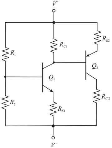
Figure 1
Calculation:
Mark the current and other parameters than redraw the circuit.
The required diagrams is shown in Figure 2
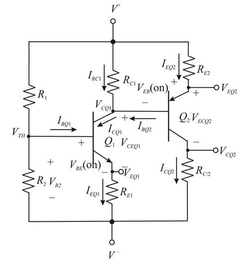
Figure 2
The value of the base current of the first transistor is calculated as,
Substitute
The value of the base current of the second transistor is calculated as,
Substitute
Apply KCL to the above circuit.
The expression for the current
Substitute
From KCL the expression for the emitter current of the second transistor is given by,
The expression to determine the voltage
The expression to determine the value of the resistance
The expression to determine the value of the collector voltage is
The expression to determine the value of the resistance
Substitute
By KCL in Figure 2 the expression for the current
Substitute
The expression to determine the value of the emitter voltage
The expression to determine the value of the resistance
Substitute
The expression for the Thevenin voltage is evaluated as,
The Thevenin equivalent base circuit is shown in Figure 3.
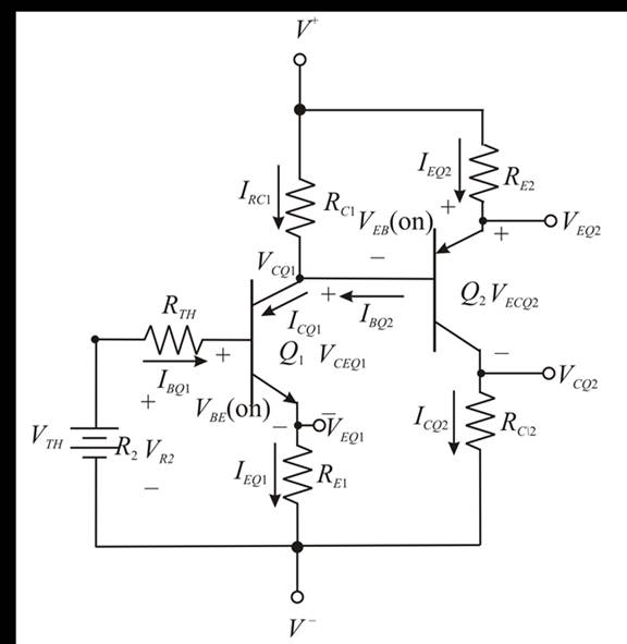
Figure 3
Apply KVL to the above circuit.
For bias stable voltage the value of the Thevenin equivalent resistance is given by,
Substitute
Substitute
Substitute
The expression to determine the value of the Thevenin equivalent resistance is given by,
Substitute
Conclusion:
Therefore, the value of the resistance required to design the circuit are
Want to see more full solutions like this?
Chapter 5 Solutions
Microelectronics Circuit Analysis and Design


- draw a qpsk modulator circuit using different circuit compents like resistors, transistors etc not a block diagramarrow_forwardIn your own words, briefly describe the basic operation of an E-MOSFET.arrow_forwardWhat is the collector-emitter voltage for thetransistor if IS = 7 × 10⁻¹⁶ μA,αF = 0.99, and αR = 0.5? (b) What is the emittercollector voltage for the transistor P5.56(b)for the same transistor parameters?arrow_forward
- What do you think is the role of transistors in circuits and electronics? Explain it throughly.arrow_forward5- a-) Define the MOSFET in the figure, explain by drawing its input and output circuit characteristics.b-) Since k=0.1 mA/V2, VGS=5V and VT=2.5V for this MOSFET, find the VDS voltage using the circuit.arrow_forwardWhat is the voltage value Vgs for the n-channel MOSFET given in the figure? (VT=2V, K=0.4mA/V^2, VDD=5V, RD=RS=1K)arrow_forward
- Fixed-bias configuration, Emitter-bias configuration, and Voltage-divider configuration- rank these three configurations based on their provided stability (i.e. ? independency)to the operating point. Use mathematical terms/equations to explain and justify yourarrow_forwardDraw the equivalent circuit for a common-emitter bipolar transistor amplifier andderive suitable formulae for the amplifier current gain, voltage gain and power gain.Neglect bias,decoupling and coupling componentsarrow_forwardDraw, Illustrate and label your schematic diagram before solving the problem. 1) Given a Fixed-Biased transistor circuit with Beta DC is 200 , voltage at common collector is +22v ,base supply voltage is +11V, Base resistor is 47kOhms , collector resistor is 390 ohms ,Voltage at Base-emitter junction is 0.7v. Determine the Q-point of collector current and Voltage at collector-emitter junction. These might be help as a guide to solve the problem.arrow_forward
- Consider the circuit of Figure 2.1 using Vcc = 12 volts, Rb = 220 kΩ and Rc = 1 kΩ. Compute the theoretical base, emitter and collector voltages. Kindly show process in solutionarrow_forwardFor the circuit in Figure 1, the transistor is biased so that ICQ is 10 mA and VCEQ is 8 V. As a starting point, let VRE be 20% of VCC. Calculate the values needed for RE and RC.Assume β is 100. Select the nearest standard values for the two resistor. Calculate for VRc, Rc, VRe, Ie, Re,arrow_forward5. In your own words, briefly describe the difference between the basic operation of a pchannel depletion-type MOSFET and p-channel Enhancement-type MOSFET.arrow_forward
 Introductory Circuit Analysis (13th Edition)Electrical EngineeringISBN:9780133923605Author:Robert L. BoylestadPublisher:PEARSON
 Delmar's Standard Textbook Of ElectricityElectrical EngineeringISBN:9781337900348Author:Stephen L. HermanPublisher:Cengage Learning
 Programmable Logic ControllersElectrical EngineeringISBN:9780073373843Author:Frank D. PetruzellaPublisher:McGraw-Hill Education
 Fundamentals of Electric CircuitsElectrical EngineeringISBN:9780078028229Author:Charles K Alexander, Matthew SadikuPublisher:McGraw-Hill Education
 Electric Circuits. (11th Edition)Electrical EngineeringISBN:9780134746968Author:James W. Nilsson, Susan RiedelPublisher:PEARSON
 Engineering ElectromagneticsElectrical EngineeringISBN:9780078028151Author:Hayt, William H. (william Hart), Jr, BUCK, John A.Publisher:Mcgraw-hill Education,