
Videos
The circuit parameters for the two-transistor current source shown inFigure 10.2(b) are
The value of
Answer to Problem 10.1EP
The values are:
Explanation of Solution
Given:
The given circuit is shown below.
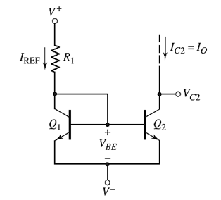
Calculation:
Apply KVL in input Loop
From equation,
From figure,
Also, both transistors are identical (
So,
Want to see more full solutions like this?
Chapter 10 Solutions
Microelectronics: Circuit Analysis and Design


- What is the voltage gain (Av) of the circuit when = 100, r0 = 40 kΩ, RB = 360 kΩ, RC = 3.3 kΩ, RE = 220 Ω, Rs = 15 kΩ and RL = 379 kΩ? NOTE-1: The output impedance r0 of the transistor will be taken into account in the calculations. NOTE-2: Capacitors are negligible at mid-band frequency.arrow_forwardVcc=25V , Vi=35mV , RB =470kΩ , RC=2,6kΩ , RE1=470Ω , RE2=1.2kΩ , RL=16.8kΩ , β=110 Find the output voltage V0 = ? Note1=Capacitors are negligible at mid-band frequency. Note2 0 The output impedance (r0) of the transistor will be neglected.arrow_forwardı just need the fınal answer Since Vcc = 20 V, RS = 3 kΩ, RB = 380 kΩ, RC = 1.2 kΩ, RE = 2.2 kΩ, RL = 911 Ω and β = 90 in the circuit in the figure, find the value of the output voltage (Vo). NOTE-1: It is within the 1 kHz mid-band frequency and the capacitors are negligible at this frequency. NOTE-2: The output impedance (r0) of the transistor will be neglected. a. 64,14 mV b. 83,88 mV c. 93,75 mV d. 74,01 mV e. 103,62 mV f. 24,67 mV g. 34,54 mV h. 49,34 mVarrow_forward
- Since Vcc = 25 V, Vi = 2 mV, RB = 470 kΩ, RC = 1.5 kΩ, RE1 = 470 Ω, RE2 = 1.2 kΩ, RL = 42 kΩ and β = 110 in the circuit in the figure, the value of the output voltage (Vo) find it. NOTE-1: Capacitors are negligible at mid-band frequency. NOTE-2: The output impedance (r0) of the transistor will be neglected.arrow_forwardFor a non -inverting operational amplifier, Rf = 80 kΩ , Ri = 6 kΩ fT = 2.35 MHz, Determine the closed loop lower critical frequency fc(cl) in kHzarrow_forwardSOLVE NUMBER 2 .1. Solve the output voltage if the gain is 24 db with aninput of 5mV.? 2. Assume a load resistor, RL of 2.2kΩs and a supply voltage of 24v. Calculate the Collector current (Ic) flowing through the load resistor when the transistor is switched fully "ON", assume Vce = 0, & β = 100. Also find the value of the Emitter resistor, Re with a voltage drop of 1.3v across it, R1, R2, and Ib. Assume also a value of 9 times Ib flowing through the resistor R2, while 10 times Ib flowing through R1.arrow_forward
- A 3-Vrms signal is fed to a transmission line whose attenuation at a certain frequency is 0.002 Neper/meter. The length of the line is 3.5 kilometers and it is terminated using an amplifier whose input and output impedances are equal to the characteristic impedance of the line. The amplifier gain is 110 dB. The output of the amplifier is connected to a similar 3.5-kilometer line. The second line is terminated by its characteristic impedance. Determine the signal voltage at the load of the second line.arrow_forwardThe common-emitter discrete amplifier shown has the following values: RB1 = 400 kΩ, RB2 = 100 kΩ, RC = 4 kΩ, RE = 500 Ω, Rsig = 1 kΩ, RL = 10 kΩ and VCC = 15 V. Assume VBE = 0.7 V and β = 90. Also assume that the capacitors are shorts for ac. The bias circuit has been analyzed and IC = 1.65 mA, Rin = 1.34 kΩ and Rout = RC. If vsig = 10 mVpeak, determine the peak value of vout.arrow_forwardFor the circuit shown, let VCC = 3.3 V, RE = 500 Ω, RC = 4 kΩ, R1 = 85 kΩ, R2 = 35 kΩ, and β = 150. Using approximation, determine the Q-point parameters: IBQ, ICQ, and VCEQ. Indicate the exact numerical values, following the given unit.arrow_forward
- In the circuit shown in the figure, Vcc = 12 V, Vin = 10 mV, β = 100, r0 = 40 kΩ, RB = 360 kΩ, RC = 3.3 kΩ, RE = 220 Ω, Rs = 0.5 kΩ and RL = 42.1 kΩ . Accordingly, find the voltage gain (Vout/Vin) of the circuit.NOTE-1: The output impedance of the transistor r0 will be taken into account in the calculations.NOTE-2: Capacitors are negligible at midband frequency.arrow_forwardIn the circuit shown in the figure, Vcc = 12 V, Vin = 10 mV, β = 100, r0 = 40 kΩ, RB = 360 kΩ, RC = 3.3 kΩ, RE = 220 Ω, Rs = 0.5 kΩ and RL = 7.1 kΩ . Accordingly, find the voltage gain (Vout/Vin) of the circuit. NOTE-1: The output impedance of the transistor r0 will be taken into account in the calculations.NOTE-2: Capacitors are negligible at midband frequency.arrow_forwardIn the circuit in the figure, Vcc = 18 V and RL = 2.2 kΩ, while C1 = C2 = CE = 0.1 μF. It is also known that for parasitic and wiring capacitors, Cwi = 15 pF, Cwo = 21 pF, Cbc = 27 pF, Cbe = 887 pF and Cce = 25 pF. Accordingly, what is the bandwidth of the system? NOTE-1: The output impedance of the transistor r0 will be neglected in the calculations. NOTE-2: The high frequency dependence of hfe, β, will be neglected.arrow_forward
 Introductory Circuit Analysis (13th Edition)Electrical EngineeringISBN:9780133923605Author:Robert L. BoylestadPublisher:PEARSON
 Delmar's Standard Textbook Of ElectricityElectrical EngineeringISBN:9781337900348Author:Stephen L. HermanPublisher:Cengage Learning
 Programmable Logic ControllersElectrical EngineeringISBN:9780073373843Author:Frank D. PetruzellaPublisher:McGraw-Hill Education
 Fundamentals of Electric CircuitsElectrical EngineeringISBN:9780078028229Author:Charles K Alexander, Matthew SadikuPublisher:McGraw-Hill Education
 Electric Circuits. (11th Edition)Electrical EngineeringISBN:9780134746968Author:James W. Nilsson, Susan RiedelPublisher:PEARSON
 Engineering ElectromagneticsElectrical EngineeringISBN:9780078028151Author:Hayt, William H. (william Hart), Jr, BUCK, John A.Publisher:Mcgraw-hill Education,