
Videos
Consider the simple MOS op−amp circuit shown in Figure P13.1. The biascurrent is
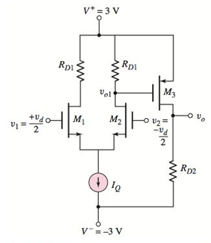
Figure P13.1
Want to see the full answer?
Check out a sample textbook solution
Chapter 13 Solutions
Microelectronics: Circuit Analysis and Design


- The transistor parameters for the differential amplifier shown in Figure P11.32 are VT N = 0.5 V, k n = 80 µA/V2, W/L = 4, and λ = 0. (a) Find RD and IQ such that ID1 = ID2 = 80 µA and vO2 = 2 V when v1 = v2 = 0. (b) Draw the dc load line, and plot the Q-point for M2. (c) What is the maximum common-mode input voltage? Figure p11.32arrow_forwardEx. 1780. A closed-loop system has sustained oscillations (i.e. constant amplitude) with a period of 85 seconds when the gains are: proportional=96, integral=0, and derivative=0. Determine the ideal- PID gains Kp, Ki (minutes^-1), Kd (minutes) using the Ziegler-Nichols method. Also determine the standard-PID values which are commonly used in industry, such as LabVIEW: Kc, Ti (min), Td (min). ans:6arrow_forwardConsider the circuit shown in FigureP13.24 . a. Find an expression for the output voltage in terms of the source current and resistance values. b. What value is the output impedance of this circuit? c. What value is the input impedance of this circuit? d.This circuit can be classified as an ideal amplifier. What is the amplifier type? (See Section11.6 for a discussion of various ideal-amplifier types.) Repeat ProblemP13.24 for the circuit shown in FigureP13.25 .arrow_forward
- Consider the bridge amplifier shown in FigureP13.62 . a. Assuming ideal op amps, derive an expression for the voltage gain vo/vs.b. If vs(t)=3 sin(ωt) sketch v1(t), v2(t), and vo(t) to scale versus time. c. If the op amps are supplied from ±15 V and clip at output voltages of ±14 V, what is the peak value of vo(t) just at the threshold of clipping?arrow_forwardConsider the circuit shown in FigureP13.9 . Sketch vin(t) and vo(t) to scale versus time. The op amp is ideal.arrow_forwardConsider the circuit shown in FigureP13.24 . a. Find an expression for the output voltage in terms of the source current and resistance values. b. What value is the output impedance of this circuit? c. What value is the input impedance of this circuit? d.This circuit can be classified as an ideal amplifier. What is the amplifier type? (See Section11.6 for a discussion of various ideal-amplifier types.)arrow_forward
- Consider the amplifier shown in FigureP13.61 . With zero dc input voltage from the signal source, it is desired that the dc output voltage be no greater than 100 mV. a. Ignoring other dc imperfections, what is the maximum offset voltage allowed for the op amp? b. Ignoring other dc imperfections, what is the maximum bias current allowed for the op amp? c. Show how to add a resistor to the circuit (including its value) so that the effects of the bias currents cancel. d. Assuming that the resistor of part (c) is in place, and ignoring offset voltage, what is the maximum offset current allowed for the op amp?arrow_forwardWithout writing or drawing tools to lean on, you must use words, not equations, graphs or schematics in your explanation. The current in a differential pair of transistors swings between the two sides of the transistor pair as the input voltage swings between the inputs. The output voltages of course follow the current inversely. Is this swing of current related to one of the chief advantages of differential operation, the elimination of common mode signals? Keep in mind, there is a restricted range of allowed current (and voltage) swing to keep the amplifier operating in a linear wayarrow_forwardDerive an expression for the voltage gain of the circuit shown in FigureP13.33 as a function of T, assuming an ideal op amp. (T varies from 0 to unity, depending on the position of the wiper of the potentiometer.)arrow_forward
- Using the parts listed in TableP13.36 , design a single-op-amp differential amplifier having a nominal differential gain of 10. Repeat ProblemP13.70 , using the instrumentation-quality circuit shown in Figure13.34 on page 677.arrow_forwardPlease assist with question 3, details on how to do. Thank you. Check image for Q3 3. Figure shows a PCM signal in which the amplitude levels of volt and volt are used to represent binary symbols 1 and 0, respectively. The code word used consists of three bits. Find the sampled version of an analog signal from which this PCM signal is derived.arrow_forwardConsider the common-source amplifier shown in Figure P11.50. The NMOS transistor has KP=50 μA/V2, L=5 μm, W=500 μm, Vto=1 V and rd=∞.a. Determine the values of IDQ, VDSQ and gm. b. Compute the voltage gain, input resistance, and output resistance, assuming that the coupling capacitors are short circuits for the ac signal. Repeat Problem P11.50 for an NMOS transistor having KP=50 μA/V2, W=600 μm, L=20 μm, Vto=2 V and rd=∞. Compare the gain with that attained in Problem P11.50.arrow_forward
 Introductory Circuit Analysis (13th Edition)Electrical EngineeringISBN:9780133923605Author:Robert L. BoylestadPublisher:PEARSON
 Delmar's Standard Textbook Of ElectricityElectrical EngineeringISBN:9781337900348Author:Stephen L. HermanPublisher:Cengage Learning
 Programmable Logic ControllersElectrical EngineeringISBN:9780073373843Author:Frank D. PetruzellaPublisher:McGraw-Hill Education
 Fundamentals of Electric CircuitsElectrical EngineeringISBN:9780078028229Author:Charles K Alexander, Matthew SadikuPublisher:McGraw-Hill Education
 Electric Circuits. (11th Edition)Electrical EngineeringISBN:9780134746968Author:James W. Nilsson, Susan RiedelPublisher:PEARSON
 Engineering ElectromagneticsElectrical EngineeringISBN:9780078028151Author:Hayt, William H. (william Hart), Jr, BUCK, John A.Publisher:Mcgraw-hill Education,