
(a)
Interpretation:
From the given pictures, the material that relates to it has to be identified.
Concept introduction:
Semiconductor: A material which can conduct electricity in range between a metal and an insulator is known as semiconductor. Addition of small amount of impurities increases conductivity of semiconductor and the process is known as doping. n-type and p-type are two types of doped semiconductors.
n-type: This is a type of doped semiconductor in which many free electrons are present in conduction band.
p-type: This is a type of doped semiconductor in which holes are present in conduction band.
Insulator: Insulators are one, in which electrons are filled in valence band with a vacant conduction band and they are parted away by band gap.
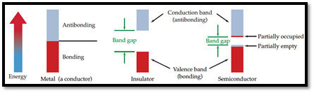
Figure 1
(b)
Interpretation:
The ascending order of electrical conductivity of given materials has to be arranged and explained.
Concept introduction:
Semiconductor: A material which can conduct electricity in range between a metal and an insulator is known as semiconductor. Addition of small amount of impurities increases conductivity of semiconductor and the process is known as doping. n-type and p-type are two types of doped semiconductors.
n-type: This is a type of doped semiconductor in which many free electrons are present in conduction band.
p-type: This is a type of doped semiconductor in which holes are present in conduction band.
Insulator: Insulators in which electrons are filled in valence band with a vacant conduction band and they are parted away by band gap. Insulators does not conduct electricity.
(c)
Interpretation:
The effect of increase in temperature on the conductivity of given material has to be given.
Concept introduction:
Semiconductor: A material which can conducts electricity in range between a metal and an insulator is known as semiconductor. Addition of small amount of impurities increases conductivity of semiconductor and the process is known as doping. n-type and p-type are two types of doped semiconductors.
n-type: This is a type of doped semiconductor in which many free electrons are present in conduction band.
p-type: This is a type of doped semiconductor in which holes are present in conduction band.
Insulator: Insulators in which electrons are filled in valence band with a vacant conduction band and they are parted away by band gap. Insulators does not conduct electricity.
Effect of change in temperature: Increase in temperature increases electrical conductivity of semiconductors because when temperature raises, there will be more electrons in conduction band and hole in valance band. On the other hand, electrical conductivity decreases when temperature increases due to increased vibrational motion of metal cation around lattice leads to disruption of flow of electrons in crystal.
Want to see the full answer?
Check out a sample textbook solution
Chapter 21 Solutions
Masteringchemistry with Pearson Etext -- Standalone Access Code Card -- For General Chemistry

- 8.97 The doping of semiconductors can be done with enough precision to tune the size of the band gap in the material. Generally, in order to have a larger band gap, the dopant should be smaller than the main material. If you are a materials engineer and need a semiconductor that has lower conductivity thin pure silicon, what clement or elements could you use as your dopant? (You do not want either an n- or a p- type material) Explain your reasoning.arrow_forward8.96 A business manager wants to provide a wider range of p- and n-type semiconductors as a strategy to enhance sales. You are the lead materials engineer assigned to communicate with this manager. How would you explain why there are more ways to build a p-type semiconductor from silicon than there are ways to build an n-type semiconductor from silicon?arrow_forwardIron titanate, FeTiO3, forms in the ilmenite crystal structure that consists of an HCP arrangement of O2- ions. (a) Which type of interstitial site will the Fe2+ ions occupy? (b) Which type of interstitial site will the Ti4+ ions occupy? (c) What fraction of the total tetrahedral sites will be occupied? (In decimal form to two places to the right of the decimal) (d) What fraction of the total octahedral sites will be occupied? (In decimal form to two places to the right of the decimal)arrow_forward
- a) A hexagonal close-packed layer in two dimensions is shown in figure 2.By identifying a suitable unit cell, calculate the packing fraction of this structure.arrow_forwardAn ideal quantum dot for use in TVs does not contain anycadmium due to concerns about disposal. One potentialmaterial for this purpose is InP, which adopts the zincblende (ZnS) structure (face-centered cubic). The unit celledge length is 5.869 Å. (a) If the quantum dot is shaped likea cube, how many of each type of atom are there in a cubiccrystal with an edge length of 3.00 nm? 5.00 nm? (b) Ifone of the nanoparticles in part (a) emits blue light and theother emits orange light, which color is emitted by the crystalwith the 3.00-nm edge length? With the 5.00-nm edgelength?arrow_forwardAn ideal quantum dot for use in TVs does not contain anycadmium due to concerns about disposal. One potentialmaterial for this purpose is InP, which adopts the zinc blende (ZnS) structure (face-centered cubic). The unit celledge length is 5.869 Å. (a) If the quantum dot is shaped likea cube, how many of each type of atom are there in a cubiccrystal with an edge length of 3.00 nm? 5.00 nm? (b) Ifone of the nanoparticles in part (a) emits blue light and theother emits orange light, which color is emitted by the crystalwith the 3.00-nm edge length? With the 5.00-nm edgelength?arrow_forward
- Which of these statements is false?(a) As you go down column 4A in the periodic table, the elementalsolids become more electrically conducting. (b) Asyou go down column 4A in the periodic table, the band gapsof the elemental solids decrease. (c) The valence electroncount for a compound semiconductor averages out to fourper atom. (d) Band gap energies of semiconductors rangefrom ∼0.1 to 3.5 eV. (e) In general, the more polar the bondsare in compound semiconductors, the smaller the band gap.arrow_forwardGraphite has a layered structure, with each layer made up of six-membered rings of carbon fused with other similar rings on all sides. The Lewis structure shows alternating single and double bonds. Diamond is an insulator, and graphite is a moderately good conductor. Explain these facts in terms of the bonding in each. (Conductance of graphite is significantly lower than metals but is higher than most nonmetals.) What behavior would you predict for carbon nanotubes, the cylindrical form of fullerenes?arrow_forwardWhat do Doped semiconductors contain?arrow_forward
- Silicon has a band gap of 1.1 eV at room temperature.(a) What wavelength of light would a photon of this energycorrespond to? (b) Draw a vertical line at this wavelength inthe figure shown, which shows the light output of the Sunas a function of wavelength. Does silicon absorb all, none,or a portion of the visible light that comes from the Sun?(c) You can estimate the portion of the overall solar spectrumthat silicon absorbs by considering the area under thecurve. If you call the area under the entire curve “100%,”what approximate percentage of the area under the curve isabsorbed by silicon?arrow_forwardA unit cell of Re03 consists of a cubic .1 arrangement of Re atoms with O atoms centred along each edge of the cube. The coordination number of each Re atom isarrow_forwardThere are four different types of band structures at 0 K. Among them, two are typified in metals, one in semiconductors and the last one in insulators. Which of the following statement/s is/are false? (i) In this band structure typified in metals, the outermost band is partially filled with electrons; (ii) In this band structure also typified in metals, there is an overlap of an empty band and a filled band; (iii) In the semiconductors, the band gap energy is narrower than insulators; (iv) In insulators, the band gap energy is wider than semiconductors. C. (iii) A. (i) E. None of the above D. (iv) B. (ii) Other:arrow_forward
 Principles of Modern ChemistryChemistryISBN:9781305079113Author:David W. Oxtoby, H. Pat Gillis, Laurie J. ButlerPublisher:Cengage Learning
 Chemistry & Chemical ReactivityChemistryISBN:9781337399074Author:John C. Kotz, Paul M. Treichel, John Townsend, David TreichelPublisher:Cengage Learning
 Chemistry & Chemical ReactivityChemistryISBN:9781133949640Author:John C. Kotz, Paul M. Treichel, John Townsend, David TreichelPublisher:Cengage Learning
 Chemistry for Engineering StudentsChemistryISBN:9781337398909Author:Lawrence S. Brown, Tom HolmePublisher:Cengage Learning
 Physical ChemistryChemistryISBN:9781133958437Author:Ball, David W. (david Warren), BAER, TomasPublisher:Wadsworth Cengage Learning,
 ChemistryChemistryISBN:9781305957404Author:Steven S. Zumdahl, Susan A. Zumdahl, Donald J. DeCostePublisher:Cengage Learning