
Videos
Consider the circuit shown in Figure P6.19 where the signal−source is
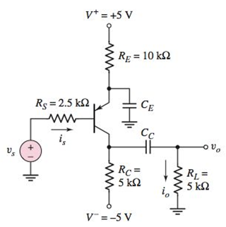
Figure P6.19
(a)
The small signal voltage gain
Answer to Problem 6.19P
The small signal voltage gain
Explanation of Solution
Given:
The sinusoidal source voltage
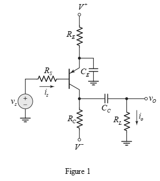
The circuit for
The current gain
The circuit parameters are shown below.
Concept used:
The expression for small signal voltage gain
The expression for transconductance is written below.
Calculation:
Apply dc analysis and KVL in base emitter
Substitute
The quiescent collector current is calculated as,
The transconductance is calculated as,
The diffusion resistance is calculated as,
Substitute
Therefore, the small signal voltage gain
The output current
Substitute
Therefore, the transconductance function
The output current is calculated as,
Therefore, the output current
The output voltage is calculated as,
Substitute
Therefore, the output voltage
Conclusion:
Thus, the small signal voltage gain
(b)
The small signal voltage gain
Answer to Problem 6.19P
The small signal voltage gain
Explanation of Solution
Given:
The current gain
Calculation:
Apply dc analysis and KVL in base emitter
Substitute
The quiescent collector current is calculated as,
The transconductance is calculated as,
The diffusion resistance is calculated as,
Substitute
Therefore, the small signal voltage gain
The output current
Substitute
Therefore, the transconductance function
The output current is calculated as,
Therefore, the output current
The output voltage is calculated as,
Substitute
Therefore, the output voltage
Conclusion:
Thus, the small signal voltage gain
Want to see more full solutions like this?
Chapter 6 Solutions
Microelectronics: Circuit Analysis and Design


- The parameters for each transistor in the circuit shown in Figure P6.75 areβ = 100 and VA = ∞. (a) Determine the small-signal parameters gm , rπ ,and ro for both transistors. (b) Determine the small-signal voltage gainAv1 = vo1/vs, assuming vo1 is connected to an open circuit, and determinethe gain Av2 = vo/vo1. (c) Determine the overall small-signal voltage gainAv = vo/vs. Compare the overall gain with the product Av1 · Av2, using thevalues calculated in part (b)arrow_forwardDescribe the combined effect of the RC circuits for higher frequency response in a BJT & FETamplifier. the subject : Analogue Electronics IIarrow_forwardCompute the transfer function of the given signal flow graph below:arrow_forward
- Describe the state-space representation of a system. How is it different from the transfer function representation, and when is it preferred?arrow_forwardCurrent and impedance levels of push-pull RF amplifier. Solid-state RF power amplifiers that provide more than 50 W or so must deal with very large currents, because the typical silicon RF BJT or PET cannot with-stand a DC collector voltage higher than about 40V. (Newer devices using materials such as silicon carbide can exceed this voltage limitation and provide greater power for the same current level.) Suppose a push-pull RF amplifier using a DC collector voltage of 36 V must provide a total peak RF output power of 200W. Typically, the AC "swing" (peak-to-peak AC excursion) of voltage at the collectors cannot exceed twice the DC power-supply voltage. (a) If each of the two devices in the push-pull amplifier delivers IOOW and has a peak-to-peak voltage of (2 x 36) = 72 V across its output terminals , what is the peak current I at the collector of each device, assuming . "d C(PK) smus01 al voltage and current? (b) At this current IC<PK >' how much series inductance L at a…arrow_forwardTrying to solve this MOSFET question but not sure how.(Given Answer:a) Av = -gm (ro|| RD)b)Av = -30.7 Ri = 20 kohm Ro = 7.67 kohm)arrow_forward
- What is the transfer function of a system, and how is it derived from a differential equation?arrow_forwardIs coupling a consequence of signal absorptions? What is the problem of this?arrow_forwardTuned Circuit Design Using a VARICAP (a) Refer to the capacitance curves for the Motorola 1N4002 The input tuning circuit of a standard analog FM radio is given below. Specify, that is design for, a voltage, capacitance, and inductance required to tune the circuit to the center frequency of KUMD-FM which operates at 103.3 MHz. Sketching and labeling a representative resonance curve is required to support your calculations. There is no single correct design answer set of values since it depends upon the voltage you initially select to tune your diode.arrow_forward
- Discuss how the circuit produces a Frequency Modulated Signalarrow_forwardKindly help to answer this figure shown. Find the transfer function of the system whose signal flow graph is shownarrow_forwardFor the NMOSFET in the circuit below, K = 4.00mA/V^2, VTHN = 1.00V, l = 0V^-1, and VIN = 4.00V.a. Solve for IDS and VOUT and verify any assumptions you made. b. Derive an equation for the small signal gain of the circuit, vout / vin as a function of the vin radian frequency, w.arrow_forward
 Introductory Circuit Analysis (13th Edition)Electrical EngineeringISBN:9780133923605Author:Robert L. BoylestadPublisher:PEARSON
 Delmar's Standard Textbook Of ElectricityElectrical EngineeringISBN:9781337900348Author:Stephen L. HermanPublisher:Cengage Learning
 Programmable Logic ControllersElectrical EngineeringISBN:9780073373843Author:Frank D. PetruzellaPublisher:McGraw-Hill Education
 Fundamentals of Electric CircuitsElectrical EngineeringISBN:9780078028229Author:Charles K Alexander, Matthew SadikuPublisher:McGraw-Hill Education
 Electric Circuits. (11th Edition)Electrical EngineeringISBN:9780134746968Author:James W. Nilsson, Susan RiedelPublisher:PEARSON
 Engineering ElectromagneticsElectrical EngineeringISBN:9780078028151Author:Hayt, William H. (william Hart), Jr, BUCK, John A.Publisher:Mcgraw-hill Education,