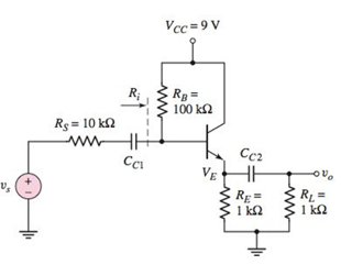
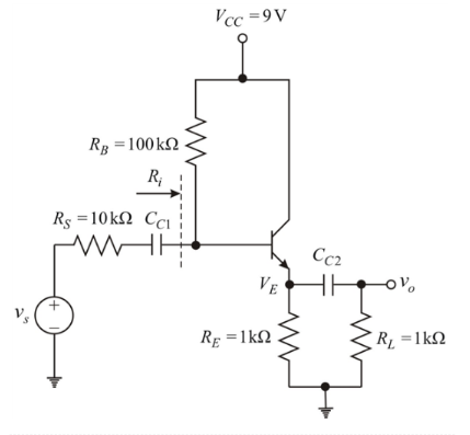
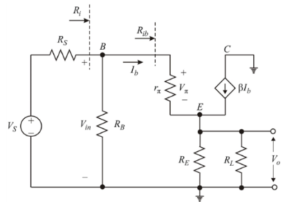
Problem 6.1EP: The circuit parameters for the circuit in Figure 6.3 are VCC=3.3V , VBB=0.850V , RB=180k , and... Problem 6.2EP: For the circuit in Figure 6.3, assume transistor parameters of =150 , VBE(on)=0.7V , and VA=150V .... Problem 6.3EP: For the circuit in Figure 6.14(a), let =90 , VA=120V , VCC=5V , VEB(on)=0.7V , RC=2.5k , RB=50k ,... Problem 6.1TYU: Using the circuit and transistor parameters given in Exercise Ex 6.1, find iB , BE , and CE for... Problem 6.2TYU: Consider the circuit in Figure 6.18. The circuit parameters are V+=3.3V , VBB=2.455V , RB=80k , and... Problem 6.4EP: Repeat Example 6.4 if the quiescent collector current is (a) ICQ=0.2mA and (b) ICQ=5mA . [Ans. (a)... Problem 6.5EP: For the circuit in Figure 6.31, let RE=0.6k , RC=5.6k , =120 , VBE(on)=0.7V , R1=250k , and R2=75k .... Problem 6.6EP Problem 6.3TYU: The parameters of the circuit shown in Figure 6.28 are VCC=5V , RC=4k , RE=0.25k , RS=0.25k ,... Problem 6.4TYU: For the circuit shown in Figure 6.31, let =100 , VBE(on)=0.7V , and VA= . Design a bias-stable... Problem 6.5TYU: Design the circuit in Figure 6.35 such that it is bias stable and the smallsignal voltage gain is... Problem 6.6TYU: For the circuit in Figure 6.28, the smallsignal voltage gain is given approximately by RC/RE . For... Problem 6.7EP: The circuit in Figure 6.38 has parameters V+=5V , V=5V , RE=4k RC=4k , RB=100k , and RS=0.5k . The... Problem 6.7TYU: For the circuit in Figure 6.39, let =125 , VBE(on)=0.7V , and VA=200V V. (a) Determine the... Problem 6.8EP: (a) Assume the circuit shown in Figure 6.40(a) is biased at IQ=0.25mA and assume transistor... Problem 6.9EP: For the circuit in Figure 6.39, let =125 , VBE(on)=0.7V , and VA=200V . Plot the dc and ac load... Problem 6.10EP: Reconsider the circuit in Figure 6.38. Let =120 , VBE(on)=0.7V , and VA= . The circuit parameters... Problem 6.11EP: For the circuit shown in Figure 6.48, let =120 , VBE(on)=0.7V , and ro= . (a) Design a biasstable... Problem 6.8TYU: For the circuit in Figure 6.31, use the parameters given in Exercise Ex 6.5. If the total... Problem 6.9TYU: Consider the circuit in Figure 6.38. Assume transistor and circuit parameters as given in Exercise... Problem 6.12EP: For the circuit shown in Figure 6.49, let VCC=12V , RE=30 , R1=1.3k , R2=4.2k , and RS=0 . The... Problem 6.13EP: Consider the circuit and transistor parameters described in Exercise Ex 6.12 for the circuit shown... Problem 6.14EP: For the circuit in Figure 6.54, the transistor parameters are: =100 , VBE(on)=0.7V , and VA=125V .... Problem 6.10TYU: Assume the circuit in Figure 6.57 uses a 2N2222 transistor. Assume a nominal dc current gain of =130... Problem 6.11TYU: For the circuit in Figure 6.58, RE=2k , R1=R2=50k and the transistor parameters are =100 ,... Problem 6.12TYU Problem 6.13TYU: For the circuit shown in Figure 6.63, the transistor parameters are: =100 , VBE(on)=0.7V , and ro= .... Problem 6.14TYU Problem 6.15TYU: For the circuit shown in Figure 6.64, let RS=0 , CB=0 , RC=RL=2k , VCC=VEE=5V , =100 , VBE(on)=0.7V... Problem 6.16TYU: Consider the circuit in Figure 6.70(a). Let =100 , VBE(on)=0.7V , and VA= for each transistor.... Problem 6.18TYU: In the circuit in Figure 6.74 the transistor parameters are: =80 , VBE(on)=0.7V , and VA= .... Problem 1RQ: Discuss, using the concept of a load line, how a simple common-emitter circuit can amplify a... Problem 2RQ Problem 3RQ Problem 4RQ: Sketch the hybrid- equivalent circuit of an npn and a pnp bipolar transistor. Problem 5RQ Problem 6RQ Problem 7RQ Problem 8RQ Problem 9RQ Problem 10RQ: Sketch a simple emitter-follower amplifier circuit and discuss the general ac circuit... Problem 11RQ: Sketch a simple common-base amplifier circuit and discuss the general ac circuit characteristics... Problem 12RQ: Compare the ac circuit characteristics of the common-emitter, emitter-follower, and common-base... Problem 13RQ Problem 14RQ Problem 6.1P: (a) Determine the smallsignal parameters gm,r , and ro of a transistor with parameters =180 and... Problem 6.2P: (a) The transistor parameters are =125 and VA=200V . A value of gm=95mA/V is desired. Determine the... Problem 6.3P: A transistor has a current gain in the range 90180 and the quiescent collector current is in the... Problem 6.4P: The transistor in Figure 6.3 has parameters =120 and VA= . The circuit parameters are VCC=3.3V ,... Problem 6.5P Problem 6.6P: For the circuit in Figure 6.3, =120 , VCC=5V , VA=100V , and RB=25k . (a) Determine VBB and RC such... Problem 6.7P: The parameters of each transistor in the circuits shown in Figure P6.7 are =120 and ICQ=0.5mA .... Problem 6.8P: The parameters of each transistor in the circuits shown in Figure P6.8 are =130 , VA=80V , and... Problem 6.9P: The circuit in Figure 6.3 is biased at VCC=10V and has a collector resistor of RC=4k . The voltage... Problem 6.10P: For the circuit in Figure 6.14, =100 , VA= , VCC=10V , and RB=50k (a) Determine VBB and RC such that... Problem 6.11P Problem 6.12P: The parameters of the transistor in the circuit in Figure P6.12 are =150 and VA= . (a) Determine R1... Problem 6.13P: Assume that =100 , VA= , R1=33k , and R2=50k for the circuit in Figure P6.13. (a) Plot the Qpoint on... Problem D6.14P: The transistor parameters for the circuit in Figure P6.13 are =100 and VA= . (a) Design the circuit... Problem D6.15P: For the circuit in Figure P6.15, the transistor parameters are =100 and VA= . Design the circuit... Problem D6.16P Problem 6.18P: The signal source in Figure P6.18 is s=5sintmV . The transistor parameters are =120 and VA= . (a)... Problem 6.19P: Consider the circuit shown in Figure P6.19 where the signalsource is s=4sintmV . (a) For transistor... Problem 6.20P Problem 6.21P: Figure P6.21 The parameters of the transistor in the circuit in Figure P6.2 1 are =100 and VA=100V .... Problem 6.22P Problem 6.23P: For the circuit in Figure P6.23, the transistor parameters are =80 and VA=80V . (a) Determine RE... Problem 6.24P: The transistor in the circuit in Figure P6.24 has parameters VBE(on)=0.7V , VA=50V , and a current... Problem 6.26P: For the transistor in the circuit in Figure P6.26, the parameters are =100 and VA= . (a) Determine... Problem 6.27P: If the collector of a transistor is connected to the base terminal, the transistor continues to... Problem 6.32P: Consider the circuit shown in Figure P6.13. Assume R1=33k and R2=50k . The transistor parameters are... Problem 6.33P: For the circuit in Figure P6.15, let =100 , VA= , RE=12.9k , and RC=6k . Determine the maximum... Problem 6.34P: Consider the circuit in Figure P6.19. The transistor parameters are =80 and VA= . (a) Determine the... Problem 6.35P: The parameters of the circuit shown in Figure P6.17 are RB=20k and RC=2.5k . The transistor... Problem 6.36P: Consider the circuit in Figure P6.26 with transistor parameters described in Problem 6.26. Determine... Problem 6.37P: For the circuit in Figure P6.20, the transistor parameters are =100 and VA=100V . The values of... Problem 6.38P: In the circuit in Figure P6.22 with transistor parameters =180 and VA= , redesign the bias resistors... Problem 6.39P: For the circuit in Figure P6.24, the transistor parameters are =100 and VA= . (a) Determine the... Problem 6.40P Problem 6.41P: Consider the ac equivalent circuit in Figure P6.40. The transistor parameters are =80 and VA= ). (a)... Problem 6.42P: For the ac equivalent circuit in Figure P6.42, RS=1k and the transistor parameters are =80 and... Problem 6.43P: The circuit and transistor parameters for the ac equivalent circuit in Figure P6.43 are RS=0.5k ,... Problem 6.45P: Consider the circuit in Figure P6.45. The transistor parameters are =120 and VA= . Repeat parts... Problem 6.47P: For the transistor in Figure P6.47, =80 and VA=150V . (a) Determine the dc voltages at the base and... Problem 6.48P: Consider the emitterfollower amplifier shown in Figure P6.48. The transistor parameters are =100 and... Problem 6.49P: The transistor parameters for the circuit in Figure P6.49 are =110 , VA=50V , and VBE(on)=0.7V . (a)... Problem 6.51P: In the circuit shown in Figure P6.51, determine the range in smallsignal voltage gain A=o/s and... Problem 6.52P: The transistor current gain in the circuit shown in Figure P6.52 is in the range 50200 . (a)... Problem 6.53P: Consider the circuit shown in Figure P6.47. The transistor current gain is in the range 100180 and... Problem 6.54P: For the circuit in Figure P6.54, the parameters are VCC=5V and RE=500 . The transistor parameters... Problem 6.59P: Figure P6.59 is an ac equivalent circuit of a commonbase amplifier. The transistor parameters are... Problem 6.60P: The transistor in the ac equivalent circuit shown in Figure P6.60 has parameters =80 and VA= .... Problem 6.61P: Consider the ac equivalent commonbase circuit shown in Figure P6.61. The transistor has parameters... Problem 6.62P Problem 6.63P: The transistor in the circuit shown in Figure P6.63 has =100 , VA= . (a) Determine the quiescent... Problem 6.64P: Repeat Problem 6.63 with a 100 resistor in series with the s , signal source. Problem 6.65P: Consider the commonbase circuit in Figure P6.65. The transistor has parameters =120 and VA= . (a)... Problem 6.66P: For the circuit shown in Figure P6.66, the transistor parameters are =100 and VA= . (a) Determine... Problem 6.67P: The parameters of the circuit in Figure P6.67 are VCC=9V , RL=4k , RC=6k , RE=3k , R1=150k , and... Problem 6.68P: For the commonbase circuit shown in Figure P6.67, letandThe transistor parameters areand(a) Design... Problem 6.69P: Consider the circuit shown in Figure P6.69. The transistor has parameters =60 and VA= . (a)... Problem D6.72P: In the circuit of Figure P6.71, let VEE=VCC=5V , =100 , VA= , RL=1k , and RS=0 . (a) Design the... Problem 6.73P: Consider the ac equivalent circuit in Figure P6.73. The transistor parameters are 1=120 , 2=80 ,... Problem 6.74P: The transistor parameters in the ac equivalent circuit shown in Figure P6.74 are 1=2=100 , VA1=VA2=... Problem 6.81P: Consider the circuit shown in Figure 6.38. The transistor parameters are given in Exercise Ex 6.7.... Problem 6.83P: For the circuit shown in Figure 6.57, the transistor parameters are =100 and VA=100V , and the... format_list_bulleted


 Introductory Circuit Analysis (13th Edition)Electrical EngineeringISBN:9780133923605Author:Robert L. BoylestadPublisher:PEARSON
 Delmar's Standard Textbook Of ElectricityElectrical EngineeringISBN:9781337900348Author:Stephen L. HermanPublisher:Cengage Learning
 Programmable Logic ControllersElectrical EngineeringISBN:9780073373843Author:Frank D. PetruzellaPublisher:McGraw-Hill Education
 Fundamentals of Electric CircuitsElectrical EngineeringISBN:9780078028229Author:Charles K Alexander, Matthew SadikuPublisher:McGraw-Hill Education
 Electric Circuits. (11th Edition)Electrical EngineeringISBN:9780134746968Author:James W. Nilsson, Susan RiedelPublisher:PEARSON
 Engineering ElectromagneticsElectrical EngineeringISBN:9780078028151Author:Hayt, William H. (william Hart), Jr, BUCK, John A.Publisher:Mcgraw-hill Education,