Microelectronics: Circuit Analysis and Design
4th Edition
ISBN: 9780073380643
Author: Donald A. Neamen
Publisher: McGraw-Hill Companies, The
bartleby

Videos

Textbook Question
Book Icon
Chapter 9, Problem 9.62P

Consider the differential amplifier shown in Figure 9.24(a). Assume thateach resistor is 50 ( 1 ± x ) k Ω . (a) Determine the worst case common-modegain A C M = v O / v C M , where v C M = v 1 = v 2 . (b) Evaluate A C M andCMRR(dB) for x = 0.01 , 0.02 , and 0.05.

(a)

Expert Solution
Check Mark
To determine

The value of the worst case common mode gain.

Answer to Problem 9.62P

The value of the worst case common mode gain is 2x1+x .

Explanation of Solution

Calculation:

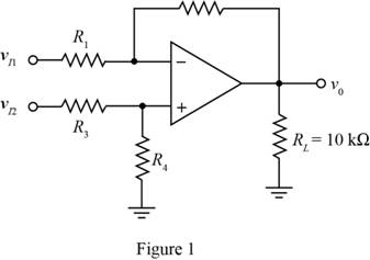
The given diagram is shown in Figure 1

  Microelectronics: Circuit Analysis and Design, Chapter 9, Problem 9.62P , additional homework tip  1

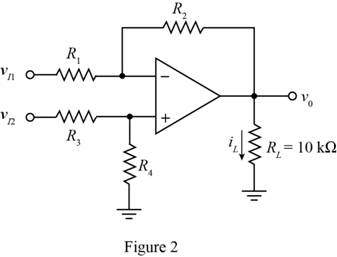
Mark the voltages and redraw the circuit.

The required diagram is shown in Figure 2

  Microelectronics: Circuit Analysis and Design, Chapter 9, Problem 9.62P , additional homework tip  2

The expression for the common mode voltage gain is given by,

  ACM=vOvCM

The expression for the value of the voltage v1 is given by,

  v1=v2

The expression for the voltage v2 by voltage division rule is given by,

  v2=(R4R3+R4)vI2

Apply KCL at the inverting terminal.

  v I1v1R1=v1vOR2v I1R2v1R1v1R1R1R2=vOR2vO=vI1( R 2 R 1 )+v1(1+ R 2 R 1 )

Substitute v2 for v1 in the above equation.

  vO=vI1(R2R1)+v2(1+R2R1)

Substitute (R4R3+R4)vI2 for v2 in the above equation.

  vO=vI1(R2R1)+(( R 4 R 3 + R 4 )vI2)(1+R2R1) …… (1)

The expression for the common node input voltage is given by,

  vCM=vI1

The expression for the common node input voltage is given by,

  vCM=vI2

Substitute vCM for vI1 and vCM for vI2 in the above equation.

  vO=vCM( R 2 R 1 )+(( R 4 R 3 + R 4 )v CM)(1+ R 2 R 1 )vOv CM=[( R 4 R 3 + R 4 )( R 1 + R 2 R 1 ) R 2 R 1]

Substitute ACM for vOvCM in the above equation.

  ACM=[( R 4 R 3 + R 4 )( R 1 + R 2 R 1 ) R 2 R 1]=R4R3+R4(1 R 2 R 3 R 1 R 4 ) …… (2)

In the above equation the worst case ACM is obtained when R4R3+R4 is maximum and 1R2R3R1R4 is minimum. The second case arises when R2 and R3R4 is minimum and R1 is maximum. The third case arises when the value of R1,R4 are minimum and R2 , R3 is minimum.

For worst condition the value of the resistance R1 is given by,

  R1=50(1+x)

For worst condition the value of the resistance R2 is given by,

  R2=50(1x)

For worst condition the value of the resistance R3 is given by,

  R3=50(1x)

For worst condition the value of the resistance R4 is given by,

  R4=50(1+x)

Substitute 50(1+x) for R1 , 50(1x) for R2 , 50(1x) for R3 and 50(1+x) for R4 in the above equation.

  ACM=50( 1+x)50( 1x)+50( 1+x)(1 ( 50( 1x ) )( 50( 1x ) ) ( 50( 1+x ) )( 50( 1+x ) ))=2x1+x …… (3)

Conclusion:

Therefore, the value of the worst case common mode gain is 2x1+x .

(b)

Expert Solution
Check Mark
To determine

The value of the CMRR and the common mode gain.

Answer to Problem 9.62P

The value of ACM for x equals to 0.01 is 0.0198 , for x equal to 0.02 is 0.0392 and for x equals to 0.05 is 0.0952 . The value of the CMRR for for x equals to 0.01 is 33.979dB , for x equal to 0.02 is 27.959dB and for x equals to 0.05 is 20dB .

Explanation of Solution

Calculation:

The expression for the common mode gain is given by,

  vCM=v I2+v I12vI1=2vCMvI2

The expression for the differential voltage is given by,

  vd=vI2vI1

Substitute 2vCMvI2 for vI1 in the above equation.

  vd=vI22vCM+vI2vd=2vI22vCMvI2=vd2+vCM

The expression for the voltage vI1 is given by,

  vI1=vCMvd2

The expression for the common mode voltage is given by,

  vCM=vI2+vI12

Substitute vCMvd2 for vI1 and vd2+vCM for vI2 in the above equation.

  vCM= v d 2+v CMv CM v d 22=0V

Substitute vCMvd2 for vI1 and vd2+vCM for vI2 in equation (1).

  vO=(vCMvd2)(R2R1)+[( R 4 R 3+ R 4)( R 1+ R 2 R 1)](vd2+vCM)

Substitute 0 for vCM in the above equation.

  vO=( v d 2)( R 2 R 1 )+[( R 4 R 3 + R 4 )( R 1 + R 2 R 1 )]( v d 2)=[( R 4 R 3 + R 4 )( R 1 + R 2 R 1 )+( R 2 R 1 )]vd2

Substitute 50(1+x) for R1 , 50(1x) for R2 , 50(1x) for R3 and 50(1+x) for R4 in the above equation.

  vO=[( 50( 1+x ) 50( 1x )+50( 1+x ))( 50( 1x )+( 50( 1+x ) ) 50( 1x ))+( 50( 1x ) 50( 1+x ))]vd2vO=[21+x]vd2vOvd=[21+x]

Substitute Ad for vOvd in the above equation.

  Ad=[11+x]

The expression for the CMRR is given by,

  CMRR(dB)=20log10|AdACM|

Substitute for 11+x for Ad and 2x1+x for ACM in the above equation.

  CMRR(dB)=20log10| 1 1+x 2x 1+x|=20log10|12x| …… (4)

Substitute 0.01 for x in equation (3).

  ACM=2( 0.01)1+0.01=0.0198

Substitute 0.01 for x in equation (4).

  CMRR(dB)=20log10|12( 0.01)|=33.979dB

Substitute 0.02 for x in equation (3).

  ACM=2( 0.02)1+0.02=0.0392

Substitute 0.02 for x in equation (4).

  CMRR(dB)=20log10|12( 0.02)|=27.959dB

Substitute 0.05 for x in equation (3).

  ACM=2( 0.05)1+0.05=0.0952

Substitute 0.05 for x in equation (4).

  CMRR(dB)=20log10|12( 0.05)|=20dB

Conclusion:

Therefore, the value of ACM for x equals to 0.01 is 0.0198 , for x equal to 0.02 is 0.0392 and for x equals to 0.05 is 0.0952 . The value of the CMRR for for x equals to 0.01 is 33.979dB , for x equal to 0.02 is 27.959dB and for x equals to 0.05 is 20dB .

Want to see more full solutions like this?

Subscribe now to access step-by-step solutions to millions of textbook problems written by subject matter experts!
Students have asked these similar questions
Figure Q1(a) shows a Class A power amplifier circuit. Given the output signal is as shown in the figure, where Vm is the peak voltage and T is the period. For all transistors, you may neglect VBE and VCE(sat) in your calculations. (i) Derive an equation for power conversion efficiency, in terms of Vm, VCC, I and RL. Hence, deduce the maximum power conversion efficiency that is achievable. (ii) Determine the worst-case average power dissipation in each transistor under normal condition (i.e. RL is not open or short)
2. The output stage of a transmitter requires, owing to supply voltage limitations, a downward impedance transformation of the antenna resistance. The load impedance is 50-Ω. Suppose we wish to deliver 3 Watts of power into such a load at 915 MHz, but the power amplifier has a maximum peak-to-peak sinusoidal voltage of only 7 Volts because of various losses and transistor breakdown problems. Design a two section L-match of low pass type to allow that 3 Watts to be delivered to the 50-Ω load. Assume that all reactive elements are ideal.
Is the system that has an input output relationship causal? O8 = 9

Chapter 9 Solutions

Microelectronics: Circuit Analysis and Design

Ch. 9 - The noninverting op-amp in Figure 9.15 has a...Ch. 9 - Use superposition to determine the output voltage...Ch. 9 - Consider the voltage-to-current converter shown in...Ch. 9 - Consider the difference amplifier in Figure...Ch. 9 - In the difference amplifier shown in Figure...Ch. 9 - For the instrumentation amplifier in Figure 9.26,...Ch. 9 - An integrator with input and output voltages that...Ch. 9 - A current source has an output impedance of...Ch. 9 - Design the voltage-to-current converter shown in...Ch. 9 - All parameters associated with the instrumentation...Ch. 9 - Design the instrumentation amplifier in Figure...Ch. 9 - An integrator is driven by the series of pulses...Ch. 9 - Consider the summing op-amp in Figure 9.40. Let...Ch. 9 - Consider the bridge circuit in Figure 9.46. The...Ch. 9 - The resistance R in the bridge circuit in Figure...Ch. 9 - Describe the ideal op-amp model and describe the...Ch. 9 - Prob. 2RQCh. 9 - Describe the operation and characteristics of the...Ch. 9 - What is the concept of virtual ground?Ch. 9 - What is the significance of a zero output...Ch. 9 - When a finite op-amp gain is taken into account,...Ch. 9 - Prob. 7RQCh. 9 - Describe the operation and characteristics of the...Ch. 9 - Describe the voltage follower. What are the...Ch. 9 - What is the input resistance of an ideal...Ch. 9 - Prob. 11RQCh. 9 - Describe the operation and characteristics of an...Ch. 9 - Describe the operation and characteristics of an...Ch. 9 - Describe the operation and characteristics of an...Ch. 9 - Assume an op-amp is ideal, except for having a...Ch. 9 - The op-amp in the circuit shown in Figure P9.2 is...Ch. 9 - An op-amp is in an open-loop configuration as...Ch. 9 - Consider the equivalent circuit of the op-amp...Ch. 9 - Consider the ideal inverting op-amp circuit shown...Ch. 9 - Assume the op-amps in Figure P9.6 are ideal. Find...Ch. 9 - Consider an ideal inverting op-amp with R2=100k...Ch. 9 - (a) Design an inverting op-amp circuit with a...Ch. 9 - Consider an ideal op-amp used in an inverting...Ch. 9 - Consider the inverting amplifier shown in Figure...Ch. 9 - (a) Design an inverting op-amp circuit with a...Ch. 9 - (a) Design an inverting op-amp circuit such that...Ch. 9 - (a) In an inverting op-amp circuit, the nominal...Ch. 9 - (a) The input to the circuit shown in Figure P9.14...Ch. 9 - Design an inverting amplifier to provide a nominal...Ch. 9 - The parameters of the two inverting op-amp...Ch. 9 - Design the cascade inverting op-amp circuit in...Ch. 9 - Design an amplifier system with three inverting...Ch. 9 - Consider the circuit shown in Figure P9.19. (a)...Ch. 9 - The inverting op-amp shown in Figure 9.9 has...Ch. 9 - (a)An op-amp with an open-loop gain of Aod=7103 is...Ch. 9 - (a) For the ideal inverting op-amp circuit with...Ch. 9 - An ideal inverting op-amp circuit is to be...Ch. 9 - For the op-amp circuit shown in Figure P9.25,...Ch. 9 - The inverting op-amp circuit in Figure 9.9 has...Ch. 9 - (a) Consider the op-amp circuit in Figure P9.27....Ch. 9 - The circuit in Figure P9.28 is similar to the...Ch. 9 - Consider the ideal inverting summing amplifier in...Ch. 9 - (a) Design an ideal inverting summing amplifier to...Ch. 9 - Design an ideal inverting summing amplifier to...Ch. 9 - Consider the summing amplifier in Figure 9.14 with...Ch. 9 - The parameters for the summing amplifier in Figure...Ch. 9 - (a) Design an ideal summing op-amp circuit to...Ch. 9 - An ideal three-input inverting summing amplifier...Ch. 9 - A summing amplifier can be used as a...Ch. 9 - Consider the circuit in Figure P9.38. (a) Derive...Ch. 9 - Consider the summing amplifier in Figure 9.14(a)....Ch. 9 - Consider the ideal noninverting op-amp circuit in...Ch. 9 - (a) Design an ideal noninverting op-amp circuit...Ch. 9 - Consider the noninverting amplifier in Figure...Ch. 9 - For the circuit in Figure P9.43, the input voltage...Ch. 9 - Determine vO as a function of vI1 and vI2 for the...Ch. 9 - Consider the ideal noninverting op-amp circuit in...Ch. 9 - (a) Derive the expression for the closed-loop...Ch. 9 - The circuit shown in Figure P9.47 can be used as a...Ch. 9 - (a) Determine the closed-loop voltage gain...Ch. 9 - For the amplifier in Figure P9.49, determine (a)...Ch. 9 - Consider the voltage-follower circuit in Figure...Ch. 9 - (a) Consider the ideal op-amp circuit shown in...Ch. 9 - (a) Assume the op-amp in the circuit in Figure...Ch. 9 - Prob. 9.53PCh. 9 - A current-to-voltage converter is shown in Figure...Ch. 9 - Figure P9.55 shows a phototransistor that converts...Ch. 9 - The circuit in Figure P9.56 is an analog voltmeter...Ch. 9 - Consider the voltage-to-current converter in...Ch. 9 - The circuit in Figure P9.58 is used to drive an...Ch. 9 - Figure P9.59 is used to calculate the resistance...Ch. 9 - Consider the op-amp difference amplifier in Figure...Ch. 9 - Consider the differential amplifier shown in...Ch. 9 - Consider the differential amplifier shown in...Ch. 9 - Let R=10k in the differential amplifier in Figure...Ch. 9 - Consider the circuit shown in Figure P9.64. (a)...Ch. 9 - The circuit in Figure P9.65 is a representation of...Ch. 9 - Consider the adjustable gain difference amplifier...Ch. 9 - Assume the instrumentation amplifier in Figure...Ch. 9 - Consider the circuit in Figure P9.68. Assume ideal...Ch. 9 - Consider the circuit in Figure P969. Assume ideal...Ch. 9 - The instrumentation amplifier in Figure 9.26 has...Ch. 9 - Design the instrumentation amplifier in Figure...Ch. 9 - All parameters associated with the instrumentation...Ch. 9 - The parameters in the integrator circuit shown in...Ch. 9 - Consider the ideal op-amp integrator. Assume the...Ch. 9 - The circuit in Figure P9.75 is a first-order...Ch. 9 - (a) Using the results of Problem 9.75, design the...Ch. 9 - The circuit shown in Figure P9.77 is a first-order...Ch. 9 - (a) Using the results of Problem 9.77, design the...Ch. 9 - Prob. 9.79PCh. 9 - Consider the circuit in Figure 9.35. The diode...Ch. 9 - In the circuit in Figure P9.81, assume that Q1 and...Ch. 9 - Consider the circuit in Figure 9.36. The diode...Ch. 9 - Design an op-amp summer to produce the output...Ch. 9 - Design an op-amp summer to produce an output...Ch. 9 - Design a voltage reference source as shown in...Ch. 9 - Consider the voltage reference circuit in Figure...Ch. 9 - Consider the bridge circuit in Figure P9.87. The...Ch. 9 - Consider the bridge circuit in Figure 9.46. The...
Knowledge Booster
Background pattern image
Electrical Engineering
Learn more about
Need a deep-dive on the concept behind this application? Look no further. Learn more about this topic, electrical-engineering and related others by exploring similar questions and additional content below.
Similar questions
SEE MORE QUESTIONS
Recommended textbooks for you
Text book image
Introductory Circuit Analysis (13th Edition)
Electrical Engineering
ISBN:9780133923605
Author:Robert L. Boylestad
Publisher:PEARSON
Text book image
Delmar's Standard Textbook Of Electricity
Electrical Engineering
ISBN:9781337900348
Author:Stephen L. Herman
Publisher:Cengage Learning
Text book image
Programmable Logic Controllers
Electrical Engineering
ISBN:9780073373843
Author:Frank D. Petruzella
Publisher:McGraw-Hill Education
Text book image
Fundamentals of Electric Circuits
Electrical Engineering
ISBN:9780078028229
Author:Charles K Alexander, Matthew Sadiku
Publisher:McGraw-Hill Education
Text book image
Electric Circuits. (11th Edition)
Electrical Engineering
ISBN:9780134746968
Author:James W. Nilsson, Susan Riedel
Publisher:PEARSON
Text book image
Engineering Electromagnetics
Electrical Engineering
ISBN:9780078028151
Author:Hayt, William H. (william Hart), Jr, BUCK, John A.
Publisher:Mcgraw-hill Education,
Nyquist 1 - what is a Nyquist diagram?; Author: John Rossiter;https://www.youtube.com/watch?v=mgIvOk9JGKY;License: Standard Youtube License