
Videos
Let
(a)
The value of the voltages
for the input voltage
Answer to Problem 9.63P
The value of the voltage
Explanation of Solution
Calculation:
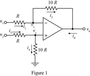
The given diagram is shown in Figure 1
The expression for the value of the voltage
Apply KCL at the node
Substitute
Apply KCL at the node
Substitute
Substitute
The expression for the current
Substitute
Substitute
Substitute
The expression for the current
Substitute
Substitute
Substitute
Substitute
Substitute
Substitute
Substitute
Substitute
Substitute
Conclusion:
Therefore, the value of the voltage
(b)
The value of the voltages
Answer to Problem 9.63P
The value of the voltage
Explanation of Solution
Calculation:
Substitute
Substitute
Substitute
Substitute
Substitute
Substitute
Substitute
Conclusion:
Therefore, the value of the voltage
(c)
The value of the voltages
Answer to Problem 9.63P
The value of the voltage
Explanation of Solution
Calculation:
Substitute
Substitute
Substitute
Substitute
Substitute
Substitute
Substitute
Conclusion:
Therefore, the value of the voltage
Want to see more full solutions like this?
Chapter 9 Solutions
Microelectronics: Circuit Analysis and Design


- 1. For an electronic device operating at a temperature of 17°C with a bandwidth of 10 kHz, determine:a. ThermalnoisepowerinwattsanddBm.b. Rmsnoisevoltagefora100Ωinternalresistance. 2. Two resistors, 20 kΩ and 50 kΩ are at ambient temperature. Calculate for a bandwidth equal to 100 kHz, the thermal noise voltage for the tworesistors connected in parallel.arrow_forwardIs the system that has an input output relationship causal? O8 = 9arrow_forwardWhy do think the output voltage ?? resembles the input sinusoid?arrow_forward
- If an amplifier’s impedance (AC Resistance) is 8 ohms, why should a speaker of 8 ohms be chosen to deliver the sound? What happens if a speaker of 4 ohms is employed instead? How about a higher impedance of 16 ohms?arrow_forwardWhen Itspice simulation of the circuit shown in the figure is performed, which of the following figures is the output representation (Vout) as given? NOTE-1: Vcc = 12 V, RO = 2.2 kO, RB 15S kO, RE 180 0 and C11 uF. NOTE-2: For the input voltage Vin, the DC offset voltage is 1.6 V, while the applied sinusoidal signal has a amplitude of 10 mV and a frequency of 10 kHz.arrow_forwardG1 = 100, G2 = 1000 and H = 0.009 for two block diagrams as open loop and closed loop given in the figure.a. Find the output voltages when the input voltage is 10 mV.b. For both systems, if G1 and G2 are doubled due to temperature increase, what will be the output voltages even though the input remains at 10 mV?c. Interpret the above results using the system's sensitivity principle.arrow_forward
- When the ltspice simulation of the circuit shown in the figure is performed, the output voltage (Vout) is obtained as given in which of the figures below? NOTE-1: Vcc = 12 V, RC = 2.2 kΩ, RB = 15 kΩ, RE = 180 Ω and C1 = 1 μF. NOTE-2: For the input voltage Vin, the DC offset voltage is 1.6 V, while the applied sinusoidal signal has a amplitude of 10 mV and a frequency of 10 kHz.arrow_forwardIf the ideal output, with a sinusoidal input signal, greatly exceeds the full-power bandwidth, what is the waveform of the output signal? Under these conditions, if the slew rate of the op amp is 10 V/μs and the frequency of the input is 1 MHz, what is the peak-to-peak amplitude of the output signal?arrow_forwardAn exponential signal has initial value Vi=v(0)=-3[V], final value Vf=(∞)=6[V], and a time constant of 10s. Determine: a) the equation for v(t) b) Graph the function for 0≤t≤100 sec, together with a table of values at 10s (or less) time intervals.arrow_forward
- What is the quality factor of varicaps? How is it determined? Its physical meaning.arrow_forwardGiven circuit, assume op-amp is ideal. What is the input resistance of the circuit, RIN? What are the currents in the inputs of op-amp? i-=? i+=? What is the output resistance of the circuit, ROUT=? Find voltage VA and VB? What is the nodal equation (KCL) at node VB? Solve for VOUT=?arrow_forwardFigure Q1(a) shows a Class A power amplifier circuit. Given the output signal is as shown in the figure, where Vm is the peak voltage and T is the period. For all transistors, you may neglect VBE and VCE(sat) in your calculations. (i) Derive an equation for power conversion efficiency, in terms of Vm, VCC, I and RL. Hence, deduce the maximum power conversion efficiency that is achievable. (ii) Determine the worst-case average power dissipation in each transistor under normal condition (i.e. RL is not open or short)arrow_forward
 Introductory Circuit Analysis (13th Edition)Electrical EngineeringISBN:9780133923605Author:Robert L. BoylestadPublisher:PEARSON
 Delmar's Standard Textbook Of ElectricityElectrical EngineeringISBN:9781337900348Author:Stephen L. HermanPublisher:Cengage Learning
 Programmable Logic ControllersElectrical EngineeringISBN:9780073373843Author:Frank D. PetruzellaPublisher:McGraw-Hill Education
 Fundamentals of Electric CircuitsElectrical EngineeringISBN:9780078028229Author:Charles K Alexander, Matthew SadikuPublisher:McGraw-Hill Education
 Electric Circuits. (11th Edition)Electrical EngineeringISBN:9780134746968Author:James W. Nilsson, Susan RiedelPublisher:PEARSON
 Engineering ElectromagneticsElectrical EngineeringISBN:9780078028151Author:Hayt, William H. (william Hart), Jr, BUCK, John A.Publisher:Mcgraw-hill Education,