
Videos
(a)
The quiescent collector currents and the dc voltage at the output.
(a)
Answer to Problem 12.36P
The value of
Explanation of Solution
Given:
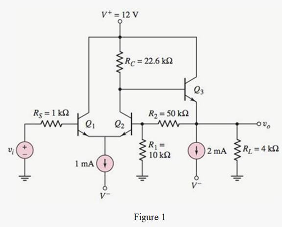
The give circuit is shown in Figure 1
Calculation:
The value of the collector current of the first transistor is calculated as,
The value of the collector current of the second transistor is calculated as,
The value of the collector voltage of the second transistor is given by,
Substitute
The expression for the output voltage is calculated as,
Substitute
The collector current of the third transistor is equal to its emitter current and is given by,
Conclusion:
Therefore, the value of
(b)
The value of the small signal voltage gain.
(b)
Answer to Problem 12.36P
The value of small signal voltage gain is
Explanation of Solution
Given:
The give circuit is shown in Figure 1

Calculation:
The expression to determine the value of the small signal input resistance of the first transistor is given by,
Substitute
The expression to determine the trans-conductance of the first transistor is given by,
Substitute
The expression to determine the value of the small signal input resistance of the second transistor is given by,
Substitute
The expression to determine the trans-conductance of the second transistor is given by,
Substitute
The expression to determine the value of the small signal input resistance of the third transistor is given by,
Substitute
The expression to determine the trans-conductance of the third transistor is given by,
Substitute
Mark the values and draw the small signal equivalent circuit.
The required diagram is shown in Figure 2
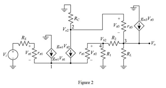
Apply KCL at the node 1
The expression to determine the input voltage is given by,
Substitute
Substitute
Substitute
Apply KCL at the node 2
Substitute
The expression to determine the value of
Apply KCL at the node 3
Substitute
Substitute
Apply KCL at the node 4
Substitute
Substitute
Substitute
The expression for the small signal voltage gain is given by,
Substitute
Conclusion:
Therefore, the value of small signal voltage gain is
Want to see more full solutions like this?
Chapter 12 Solutions
Microelectronics: Circuit Analysis and Design


- Find the range of K using the Routh - Hurwitz method for the closed - loop stability of the negative unit feedback system given the open - loop transition function belowarrow_forwardWhy negative feedback is applied in high gain amplifiers? Discuss the principles of negative voltage feedback in amplifiers with a neat diagram.arrow_forwardCalculate the feedback gain AF value. RİF=? ROF=?arrow_forward
 Introductory Circuit Analysis (13th Edition)Electrical EngineeringISBN:9780133923605Author:Robert L. BoylestadPublisher:PEARSON
 Delmar's Standard Textbook Of ElectricityElectrical EngineeringISBN:9781337900348Author:Stephen L. HermanPublisher:Cengage Learning
 Programmable Logic ControllersElectrical EngineeringISBN:9780073373843Author:Frank D. PetruzellaPublisher:McGraw-Hill Education
 Fundamentals of Electric CircuitsElectrical EngineeringISBN:9780078028229Author:Charles K Alexander, Matthew SadikuPublisher:McGraw-Hill Education
 Electric Circuits. (11th Edition)Electrical EngineeringISBN:9780134746968Author:James W. Nilsson, Susan RiedelPublisher:PEARSON
 Engineering ElectromagneticsElectrical EngineeringISBN:9780078028151Author:Hayt, William H. (william Hart), Jr, BUCK, John A.Publisher:Mcgraw-hill Education,