Microelectronics: Circuit Analysis and Design
4th Edition
ISBN: 9780073380643
Author: Donald A. Neamen
Publisher: McGraw-Hill Companies, The
bartleby

Concept explainers

bartleby

Videos

Question
Book Icon
Chapter 12, Problem 12.42P
To determine

The value of the closed loop small signal voltage gain at the mid band frequency.

Expert Solution & Answer
Check Mark

Answer to Problem 12.42P

Thevalue of the small signal closed loop voltage gain is 45.4 .

Explanation of Solution

Given:

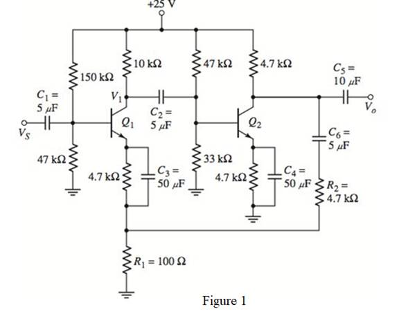
The given circuit is shown in Figure 1.

  Microelectronics: Circuit Analysis and Design, Chapter 12, Problem 12.42P , additional homework tip  1

Calculation:

The Thevenin resistance of the above circuit is calculated as,

  RTH1=(150kΩ)||(47kΩ)=( 150kΩ)( 47kΩ)( 150kΩ)+( 47kΩ)=35.8kΩ

The expression to determine the value of the Thevenin voltage is given by,

  VTH1=25V( 47kΩ 150kΩ+47kΩ)=5.96V

The expression to determine the value of the current IB1 is given by,

  IB1=VTH1VBE( on)Q1RTH1+(h FE+1)(4.7kΩ+100Ω)

Substitute 0.7V for VBE(on)Q1 , 5.96V for VTH1 , 35.8kΩ for RTH1 and 50 for hFE in the above equation.

  IB1=5.96V0.7V35.8kΩ+( 50+1)( 4.7kΩ+100Ω)=0.0187mA

The expression to determine the value of the collector current is given by,

  IC1=hFEIB1

Substitute 0.0187mA for IB1 and 50 for hFE in the above equation.

  IC1=50(0.0187mA)=0.935mA

The expression for the small signal input resistance is given by,

  rπ1=hFEVTICQ1

Substitute 50 for hFE , 0.026 for VT and 0.935mA for IC1 in the above equation.

  rπ1=( 50)( 0.026V)0.935mA=1.39kΩ

The expression for the trans-conductance of the first transistor is given by,

  gm1=ICQ1VT

Substitute 0.935mA for IC1 and 0.026V for VT in the above equation.

  gm1=0.935mA0.026V=35.96mA/V

The Thevenin resistance of the second transistor is calculated as.

  RTH2=( 47kΩ)( 33kΩ)( 47kΩ)+( 33kΩ)=19.4kΩ

The expression to determine the value of the Thevenin voltage of the second transistor is given by,

  VTH2=25V( 33kΩ 33kΩ+47kΩ)=10.3V

The expression to determine the value of the current IB1 is given by,

  IB2=VTH2VBE( on)Q1RTH2+(h FE+1)(4.7kΩ)

Substitute 0.7V for VBE(on)Q1 , 10.3V for VTH2 , 19.4kΩ for RTH2 and 50 for hFE in the above equation.

  IB2=10.3V0.7V19.4kΩ+( 50+1)( 4.7kΩ)=0.03705mA

The expression to determine the value of the collector current is given by,

  IC2=hFEIB2

Substitute 0.03705mA for IB2 and 50 for hFE in the above equation.

  IC2=50(0.03705mA)=1.85mA

The expression for the small signal input resistance is given by,

  rπ2=hFEVTIC2

Substitute 50 for hFE , 0.026 for VT and 1.85mA for IC2 in the above equation.

  rπ2=( 50)( 0.026V)1.85mA=0.703kΩ

The expression for the trans-conductance of the first transistor is given by,

  gm2=IC2VT

Substitute 1.85mA for IC2 and 0.026V for VT in the above equation.

  gm2=1.85mA0.026V=71.15mA/V

The diagram for the small signal equivalent circuit is shown in Figure 2
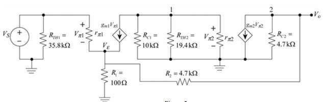
  Microelectronics: Circuit Analysis and Design, Chapter 12, Problem 12.42P , additional homework tip  2

Figure 2

The expression to determine the value of the supply voltage is given by,

  VS=Vπ1+Vε ……. (1)

Apply KCL at node ε .

  Vπ1rπ1+gm1Vπ1=VεR1VεVOR2

Substitute VSVπ1 for Vε in the above equation.

  V π1r π1+gm1Vπ1=VSV π1R1VSV π1VOR2V π1r π1+gm1Vπ1=(VSV π1)(1 R 1 +1 R 2 )VOR2

Substitute 1.39kΩ for rπ1 , 35.96mA/V for gm1 , 100Ω for R1 and 4.7kΩ for R2 in the above equation.

  V π11.39kΩ+(35.96mA/V)Vπ1=(VSV π1)(1 100Ω+1 4.7kΩ)VO4.7kΩ46.89×10³Vπ1=10.213×10³VS0.2128×103VOVπ1=0.2178VS(4.538× 10 3)VO

Apply KCL at node 1

  gm1Vπ1+Vπ210kΩ+Vπ2RTH2+Vπ2rπ2=0

Substitute 0.703kΩ for rπ2 , 35.96mA/V for gm1 and 19.4kΩ for RTH2 in the above equation.

  (35.96mA/V)Vπ1+V π210kΩ+V π2R TH2+V π20.703kΩ=0Vπ2=22.85×10³Vπ1

Apply KCL at node 2

  gm2Vπ2+VORC2+VOVεR2=0

Substitute VSVπ1 for Vε in the above equation.

  gm2Vπ2+VORC2+VO(VSV π1)R2=0

Substitute 4.7kΩ for RC2 , 71.15mA/V for gm2 and 4.7kΩ for R2 .in the above equation.

  (71.15mA/V)Vπ2+VO4.7kΩ+VO( V S V π1 )4.7kΩ=0[( 71.15 mA/V ) V π2+ V O( 0.4255× 10 3 )( 0.2128× 10 3 ) V S+( 0.2128× 10 3 ) V π1]=0

Substitute 22.85×10³Vπ1 for Vπ2 in the above equation.

  [( 71.15 mA/V )( 22.85× 10 3 V π1 )+ V O( 0.4255× 10 3 )( 0.2128× 10 3 ) V S+( 0.2128× 10 3 ) V π1]=01625.3Vπ1+VO0.42550.2128VS=0

Substitute 0.2178VS(4.538×10³)VO for Vπ1 in the above equation.

  1625.3(0.2178VS( 4.538× 10 3 )VO)+VO0.42550.2128VS=0VOVS=45.4

Conclusion:

Therefore, the value of the small signal closed loop voltage gain is 45.4 .

Want to see more full solutions like this?

Subscribe now to access step-by-step solutions to millions of textbook problems written by subject matter experts!
Students have asked these similar questions
What is the relationship between duty cycle and gain bandwidth?
What is the unity gain frequency and phase margin? (pls answer asap)
a) Determine its transfer function, C/R, using Block Diagram Reduction and Block Diagram Algebra. b) Convert it into an equivalent Signal Flow Graph and compute its error ratio, E/R, using Mason’s Gain Formula.

Chapter 12 Solutions

Microelectronics: Circuit Analysis and Design

Ch. 12 - Prob. 12.5TYUCh. 12 - Consider the noninverting op-amp circuit shown in...Ch. 12 - Design a feedback voltage amplifier to provide a...Ch. 12 - Prob. 12.6TYUCh. 12 - (a) Assume the transistor in the source-follower...Ch. 12 - Consider the common-base circuit in Figure...Ch. 12 - Design a feedback current amplifier to provide a...Ch. 12 - Prob. 12.8TYUCh. 12 - Prob. 12.9TYUCh. 12 - For the circuit in Figure 12.31, the transistor...Ch. 12 - Design a transconductance feedback amplifier with...Ch. 12 - Prob. 12.10TYUCh. 12 - Consider the circuit in Figure 12.39, with...Ch. 12 - Consider the BJT feedback circuit in Figure...Ch. 12 - Prob. 12.12TYUCh. 12 - Consider the circuit in Figure...Ch. 12 - Prob. 12.16EPCh. 12 - Prob. 12.17EPCh. 12 - Consider the circuit in Figure 12.44(a) with...Ch. 12 - Consider the circuit in Figure 12.16 with the...Ch. 12 - Prob. 12.18EPCh. 12 - Consider the loop gain function T(f)=(3000)(1+jf...Ch. 12 - Consider the loop gain function given in Exercise...Ch. 12 - Prob. 12.16TYUCh. 12 - Prob. 12.17TYUCh. 12 - Prob. 12.20EPCh. 12 - Prob. 12.21EPCh. 12 - Prob. 12.22EPCh. 12 - What are the two general types of feedback and...Ch. 12 - Prob. 2RQCh. 12 - Prob. 3RQCh. 12 - Prob. 4RQCh. 12 - Prob. 5RQCh. 12 - Prob. 6RQCh. 12 - Describe the series and shunt output connections...Ch. 12 - Describe the effect of a series or shunt input...Ch. 12 - Describe the effect of a series or shunt output...Ch. 12 - Consider a noninverting op-amp circuit. Describe...Ch. 12 - Prob. 11RQCh. 12 - What is the Nyquist stability criterion for a...Ch. 12 - Using Bode plots, describe the conditions of...Ch. 12 - Prob. 14RQCh. 12 - Prob. 15RQCh. 12 - Prob. 16RQCh. 12 - Prob. 17RQCh. 12 - (a) A negative-feedback amplifier has a...Ch. 12 - Prob. 12.2PCh. 12 - The ideal feedback transfer function is given by...Ch. 12 - Prob. 12.4PCh. 12 - Consider the feedback system shown in Figure 12.1...Ch. 12 - The open-loop gain of an amplifier is A=5104. If...Ch. 12 - Two feedback configurations are shown in Figures...Ch. 12 - Three voltage amplifiers are in cascade as shown...Ch. 12 - (a) The open-loop low-frequency voltage gain of an...Ch. 12 - (a) Determine the closed-loop bandwidth of a...Ch. 12 - (a) An inverting amplifier uses an op-amp with an...Ch. 12 - The basic amplifier in a feedback configuration...Ch. 12 - Consider the two feedback networks shown in...Ch. 12 - Prob. 12.14PCh. 12 - Two feedback configurations are shown in Figures...Ch. 12 - Prob. 12.16PCh. 12 - The parameters of the ideal series-shunt circuit...Ch. 12 - For the noninverting op-amp circuit in Figure...Ch. 12 - Consider the noninverting op-amp circuit in Figure...Ch. 12 - The circuit parameters of the ideal shunt-series...Ch. 12 - Consider the ideal shunt-series amplifier shown in...Ch. 12 - Consider the op-amp circuit in Figure P12.22. The...Ch. 12 - An op-amp circuit is shown in Figure P12.22. Its...Ch. 12 - Prob. 12.24PCh. 12 - Prob. 12.25PCh. 12 - Consider the circuit in Figure P12.26. The input...Ch. 12 - The circuit shown in Figure P12.26 has the same...Ch. 12 - The circuit parameters of the ideal shunt-shunt...Ch. 12 - Prob. 12.29PCh. 12 - Consider the current-to-voltage converter circuit...Ch. 12 - Prob. 12.31PCh. 12 - Determine the type of feedback configuration that...Ch. 12 - Prob. 12.33PCh. 12 - A compound transconductance amplifier is to be...Ch. 12 - The parameters of the op-amp in the circuit shown...Ch. 12 - Prob. 12.36PCh. 12 - Consider the series-shunt feedback circuit in...Ch. 12 - The circuit shown in Figure P12.38 is an ac...Ch. 12 - Prob. 12.39PCh. 12 - Prob. 12.40PCh. 12 - Prob. 12.41PCh. 12 - Prob. 12.42PCh. 12 - Prob. D12.43PCh. 12 - Prob. D12.44PCh. 12 - An op-amp current gain amplifier is shown in...Ch. 12 - Prob. 12.46PCh. 12 - Prob. 12.47PCh. 12 - Prob. 12.48PCh. 12 - The circuit in Figure P 12.49 has transistor...Ch. 12 - (a) Using the small-signal equivalent circuit in...Ch. 12 - The circuit in Figure P12.51 is an example of a...Ch. 12 - Prob. 12.52PCh. 12 - For the transistors in the circuit in Figure P...Ch. 12 - Consider the transconductance amplifier shown in...Ch. 12 - Consider the transconductance feedback amplifier...Ch. 12 - Prob. 12.57PCh. 12 - Prob. D12.58PCh. 12 - Prob. 12.59PCh. 12 - Prob. D12.60PCh. 12 - Prob. 12.61PCh. 12 - The transistor parameters for the circuit shown in...Ch. 12 - Prob. 12.63PCh. 12 - For the circuit in Figure P 12.64, the transistor...Ch. 12 - Prob. 12.65PCh. 12 - Prob. 12.66PCh. 12 - Design a feedback transresistance amplifier using...Ch. 12 - Prob. 12.68PCh. 12 - Prob. 12.69PCh. 12 - Prob. 12.70PCh. 12 - The transistor parameters for the circuit shown in...Ch. 12 - Prob. 12.72PCh. 12 - The open-loop voltage gain of an amplifier is...Ch. 12 - A loop gain function is given by T(f)=( 103)(1+jf...Ch. 12 - A three-pole feedback amplifier has a loop gain...Ch. 12 - A three-pole feedback amplifier has a loop gain...Ch. 12 - A feedback system has an amplifier with a...Ch. 12 - Prob. 12.78PCh. 12 - Prob. 12.79PCh. 12 - Consider a feedback amplifier for which the...Ch. 12 - Prob. 12.81PCh. 12 - A feedback amplifier has a low-frequency open-loop...Ch. 12 - Prob. 12.83PCh. 12 - A loop gain function is given by T(f)=500(1+jf 10...Ch. 12 - Prob. 12.85PCh. 12 - Prob. 12.86PCh. 12 - Prob. 12.87PCh. 12 - Prob. 12.88PCh. 12 - The amplifier described in Problem 12.82 is to be...Ch. 12 - Prob. 12.90PCh. 12 - Prob. 12.91CSPCh. 12 - Prob. 12.93CSPCh. 12 - Prob. 12.94CSPCh. 12 - Prob. D12.95DPCh. 12 - Op-amps with low-frequency open-loop gains of 5104...Ch. 12 - Prob. D12.97DP
Knowledge Booster
Background pattern image
Electrical Engineering
Learn more about
Need a deep-dive on the concept behind this application? Look no further. Learn more about this topic, electrical-engineering and related others by exploring similar questions and additional content below.
Similar questions
SEE MORE QUESTIONS
Recommended textbooks for you
Text book image
Introductory Circuit Analysis (13th Edition)
Electrical Engineering
ISBN:9780133923605
Author:Robert L. Boylestad
Publisher:PEARSON
Text book image
Delmar's Standard Textbook Of Electricity
Electrical Engineering
ISBN:9781337900348
Author:Stephen L. Herman
Publisher:Cengage Learning
Text book image
Programmable Logic Controllers
Electrical Engineering
ISBN:9780073373843
Author:Frank D. Petruzella
Publisher:McGraw-Hill Education
Text book image
Fundamentals of Electric Circuits
Electrical Engineering
ISBN:9780078028229
Author:Charles K Alexander, Matthew Sadiku
Publisher:McGraw-Hill Education
Text book image
Electric Circuits. (11th Edition)
Electrical Engineering
ISBN:9780134746968
Author:James W. Nilsson, Susan Riedel
Publisher:PEARSON
Text book image
Engineering Electromagnetics
Electrical Engineering
ISBN:9780078028151
Author:Hayt, William H. (william Hart), Jr, BUCK, John A.
Publisher:Mcgraw-hill Education,
Understanding Amplitude Modulation; Author: Rohde Schwarz;https://www.youtube.com/watch?v=I46eP8uZh_Y;License: Standard Youtube License