Microelectronics: Circuit Analysis and Design
4th Edition
ISBN: 9780073380643
Author: Donald A. Neamen
Publisher: McGraw-Hill Companies, The
bartleby

Videos

Textbook Question
Book Icon
Chapter 12, Problem 12.53P

For the transistors in the circuit in Figure P 12.53, the parameters are: h F E = 50 , V B E ( on ) = 0.7 V , and V A = . Using nodal analysis, determine the closed-loop current gain A i f = i o / i s .

Chapter 12, Problem 12.53P, For the transistors in the circuit in Figure P 12.53, the parameters are: hFE=50,VBE(on)=0.7V, and

Expert Solution & Answer
Check Mark
To determine

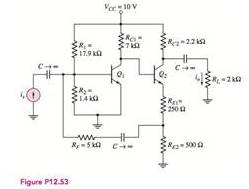
The value of the closed loop current gain of the circuit.

Answer to Problem 12.53P

The value of the current gain is 5.33 .

Explanation of Solution

Given:

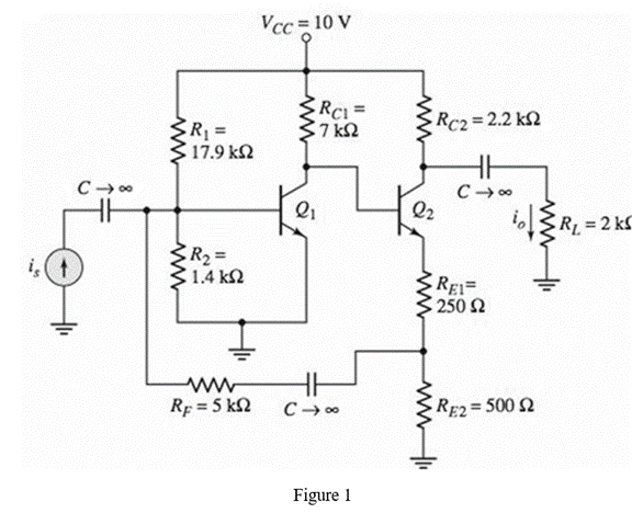
The given diagram is shown in Figure 1

  Microelectronics: Circuit Analysis and Design, Chapter 12, Problem 12.53P , additional homework tip  1

Calculation:

The small signal model of the above circuit is shown below.

The required diagram is shown in Figure 2

  Microelectronics: Circuit Analysis and Design, Chapter 12, Problem 12.53P , additional homework tip  2

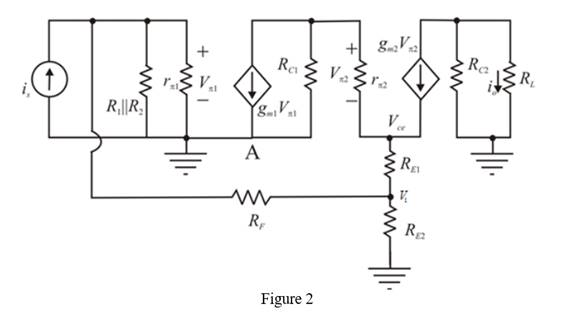
The expression to determine the value of the Thevenin resistance of the circuit is given by,

  RTH=( 1.4kΩ)( 17.9kΩ)( 1.4kΩ)+( 17.9kΩ)=1.298kΩ

The Thevenin voltage of the circuit is calculated as,

  VTH=( 1.4kΩ 1.4kΩ+17.9kΩ)10V=0.725V

The expression for the base current of the first transistor is given by,

  IB1=VTHVBE(on)RTH

Substitute 1.298kΩ for RTH , 0.7V for VBE(on) , and 0.725V for VTH in the above equation.

  IB1=0.725V0.7V1.298kΩ=0.0196mA

The expression to determine the collector current of the first transistor is given by,

  IC1=hFEIB1

Substitute 50 for hFE and 0.0196mA for IB1 in the above equation.

  IC1=50(0.0196mA)=0.98mA

The expression to determine the value of the base voltage of the second transistor is given by,

  VB2=10VIC1(7kΩ)

Substitute 0.98mA for IC1 in the above equation.

  VB2=10V(0.98mA)(7kΩ)=3.14V

The expression for the current IE2 is given by,

  IE2=VB2VBE(on)250Ω+250Ω

Substitute 3.14V for VB2 and 0.7V for VBE(on) in the above equation.

  IE2=3.14V0.7V250Ω+250Ω=3.25mA

The expression to determine the value of the collector current IC2 is given by,

  IC2=IE2(h FE1+h FE)

Substitute 3.25mA for IE2 and 50 for hFE in the above equation.

  IC2=(3.25mA)( 50 1+50)=3.19mA

The expression for the transconductance of the first transistor is given by,

  gm1=IC10.026V

Substitute 0.98mA for IC1 in the above equation.

  gm1=0.98mA0.026V=37.7mA/V

The expression for the small signal resistance is given by,

  rπ1=hFEgm1

Substitute 50 for hFE and 37.7mA/V for gm1 in the above equation.

  rπ1=5037.7mA/V=1.33kΩ

The expression for the transconductance of the second transistor is given by,

  gm2=IC20.026V

Substitute 3.19mA for IC2 in the above equation.

  gm2=3.19mA0.026V=123mA/V

The expression for the small signal resistance is given by,

  rπ2=hFEgm2

Substitute 120 for hFE and 123mA/V for gm2 in the above equation.

  rπ2=120123mA/V=0.408kΩ

Apply KCL at source iS .

  iS=Vπ11.4kΩ||1.79kΩ||rπ1+Vπ1V15kΩ

Substitute 1.33kΩ for rπ1 in the above equation.

  iS=V π11.4kΩ||1.79kΩ||1.33kΩ+V π1V15kΩ=1.722Vπ10.20V1 …… (1)

Apply KCL at node A.

  gm1Vπ1+Vπ2rπ2+Vπ2+VCE7kΩ=0

Substitute 37.7mA/V for gm1 and 0.408kΩ for rπ2 in the above equation.

  (37.7mA/V)Vπ1+V π20.408kΩ+V π2+V CE7kΩ=037.7Vπ1+2.594Vπ2+0.1429VCE=0 …… (2)

Apply KCL at node VCE .

  Vπ2rπ2+gm2Vπ2+VCEV1250Ω=0

Substitute 123mA/V for gm2 and 0.408kΩ for rπ2 in the above equation.

  V π20.408kΩ+(123mA/V)Vπ2+V CEV1250Ω=0125.5Vπ2=4VCE4V1 ……… (3)

Apply KCL at V1 .

  V CEV1250Ω=V1500Ω+V1V π15kΩVCE=1.55V10.05Vπ1

Substitute 1.55V10.05Vπ1 for VCE in equation (3).

  37.7Vπ1+2.594Vπ2+0.1429(1.55V10.05V π1)=0125.5Vπ2=2.20V10.20Vπ1 …… (4)

Substitute 1.55V10.05Vπ1 for VCE in equation (2).

  37.7Vπ1+2.594Vπ2+0.1429(1.55V10.05V π1)=0V1=170.16Vπ1+11.71Vπ2

Substitute 170.16Vπ1+11.71Vπ2 for V1 in equation (1).

  iS=1.722Vπ10.20(170.16V π1+11.71V π2)=35.75Vπ1+2.342Vπ2 ……. (5)

Substitute 170.16Vπ1+11.71Vπ2 for V1 in equation (4).

  125.5Vπ2=2.20(170.16V π1+11.71V π2)0.20Vπ1Vπ1=0.4040Vπ2

Substitute 0.4040Vπ2 for Vπ1 in equation (5).

  iS=35.75(0.4040V π2)+2.342(V π2)=12.10Vπ2 ….. (6)

The expression to determine the value of the output current is given by,

  iO=gm2Vπ2(2.2kΩ2.2kΩ+2kΩ)

Substitute and 123mA/V for gm2 in the above equation.

  iO=(123mA/V)Vπ2( 2.2kΩ 2.2kΩ+2kΩ)Vπ2=0.01552iO

Substitute 0.01552iO for Vπ1 in equation (6).

  iS=12.10(0.01552iO)iSiO=5.33

Conclusion:

Therefore, the value of the current gain is 5.33 .

Want to see more full solutions like this?

Subscribe now to access step-by-step solutions to millions of textbook problems written by subject matter experts!
Students have asked these similar questions
Discuss the distinction between open-loop gain and closed-loop gain.
Use feedback theory to derive an expression for the input impedance of the “shunt-shunt” feedback amplifier as shown.
What are the advantages of positive feedback amplifier?

Chapter 12 Solutions

Microelectronics: Circuit Analysis and Design

Ch. 12 - Prob. 12.5TYUCh. 12 - Consider the noninverting op-amp circuit shown in...Ch. 12 - Design a feedback voltage amplifier to provide a...Ch. 12 - Prob. 12.6TYUCh. 12 - (a) Assume the transistor in the source-follower...Ch. 12 - Consider the common-base circuit in Figure...Ch. 12 - Design a feedback current amplifier to provide a...Ch. 12 - Prob. 12.8TYUCh. 12 - Prob. 12.9TYUCh. 12 - For the circuit in Figure 12.31, the transistor...Ch. 12 - Design a transconductance feedback amplifier with...Ch. 12 - Prob. 12.10TYUCh. 12 - Consider the circuit in Figure 12.39, with...Ch. 12 - Consider the BJT feedback circuit in Figure...Ch. 12 - Prob. 12.12TYUCh. 12 - Consider the circuit in Figure...Ch. 12 - Prob. 12.16EPCh. 12 - Prob. 12.17EPCh. 12 - Consider the circuit in Figure 12.44(a) with...Ch. 12 - Consider the circuit in Figure 12.16 with the...Ch. 12 - Prob. 12.18EPCh. 12 - Consider the loop gain function T(f)=(3000)(1+jf...Ch. 12 - Consider the loop gain function given in Exercise...Ch. 12 - Prob. 12.16TYUCh. 12 - Prob. 12.17TYUCh. 12 - Prob. 12.20EPCh. 12 - Prob. 12.21EPCh. 12 - Prob. 12.22EPCh. 12 - What are the two general types of feedback and...Ch. 12 - Prob. 2RQCh. 12 - Prob. 3RQCh. 12 - Prob. 4RQCh. 12 - Prob. 5RQCh. 12 - Prob. 6RQCh. 12 - Describe the series and shunt output connections...Ch. 12 - Describe the effect of a series or shunt input...Ch. 12 - Describe the effect of a series or shunt output...Ch. 12 - Consider a noninverting op-amp circuit. Describe...Ch. 12 - Prob. 11RQCh. 12 - What is the Nyquist stability criterion for a...Ch. 12 - Using Bode plots, describe the conditions of...Ch. 12 - Prob. 14RQCh. 12 - Prob. 15RQCh. 12 - Prob. 16RQCh. 12 - Prob. 17RQCh. 12 - (a) A negative-feedback amplifier has a...Ch. 12 - Prob. 12.2PCh. 12 - The ideal feedback transfer function is given by...Ch. 12 - Prob. 12.4PCh. 12 - Consider the feedback system shown in Figure 12.1...Ch. 12 - The open-loop gain of an amplifier is A=5104. If...Ch. 12 - Two feedback configurations are shown in Figures...Ch. 12 - Three voltage amplifiers are in cascade as shown...Ch. 12 - (a) The open-loop low-frequency voltage gain of an...Ch. 12 - (a) Determine the closed-loop bandwidth of a...Ch. 12 - (a) An inverting amplifier uses an op-amp with an...Ch. 12 - The basic amplifier in a feedback configuration...Ch. 12 - Consider the two feedback networks shown in...Ch. 12 - Prob. 12.14PCh. 12 - Two feedback configurations are shown in Figures...Ch. 12 - Prob. 12.16PCh. 12 - The parameters of the ideal series-shunt circuit...Ch. 12 - For the noninverting op-amp circuit in Figure...Ch. 12 - Consider the noninverting op-amp circuit in Figure...Ch. 12 - The circuit parameters of the ideal shunt-series...Ch. 12 - Consider the ideal shunt-series amplifier shown in...Ch. 12 - Consider the op-amp circuit in Figure P12.22. The...Ch. 12 - An op-amp circuit is shown in Figure P12.22. Its...Ch. 12 - Prob. 12.24PCh. 12 - Prob. 12.25PCh. 12 - Consider the circuit in Figure P12.26. The input...Ch. 12 - The circuit shown in Figure P12.26 has the same...Ch. 12 - The circuit parameters of the ideal shunt-shunt...Ch. 12 - Prob. 12.29PCh. 12 - Consider the current-to-voltage converter circuit...Ch. 12 - Prob. 12.31PCh. 12 - Determine the type of feedback configuration that...Ch. 12 - Prob. 12.33PCh. 12 - A compound transconductance amplifier is to be...Ch. 12 - The parameters of the op-amp in the circuit shown...Ch. 12 - Prob. 12.36PCh. 12 - Consider the series-shunt feedback circuit in...Ch. 12 - The circuit shown in Figure P12.38 is an ac...Ch. 12 - Prob. 12.39PCh. 12 - Prob. 12.40PCh. 12 - Prob. 12.41PCh. 12 - Prob. 12.42PCh. 12 - Prob. D12.43PCh. 12 - Prob. D12.44PCh. 12 - An op-amp current gain amplifier is shown in...Ch. 12 - Prob. 12.46PCh. 12 - Prob. 12.47PCh. 12 - Prob. 12.48PCh. 12 - The circuit in Figure P 12.49 has transistor...Ch. 12 - (a) Using the small-signal equivalent circuit in...Ch. 12 - The circuit in Figure P12.51 is an example of a...Ch. 12 - Prob. 12.52PCh. 12 - For the transistors in the circuit in Figure P...Ch. 12 - Consider the transconductance amplifier shown in...Ch. 12 - Consider the transconductance feedback amplifier...Ch. 12 - Prob. 12.57PCh. 12 - Prob. D12.58PCh. 12 - Prob. 12.59PCh. 12 - Prob. D12.60PCh. 12 - Prob. 12.61PCh. 12 - The transistor parameters for the circuit shown in...Ch. 12 - Prob. 12.63PCh. 12 - For the circuit in Figure P 12.64, the transistor...Ch. 12 - Prob. 12.65PCh. 12 - Prob. 12.66PCh. 12 - Design a feedback transresistance amplifier using...Ch. 12 - Prob. 12.68PCh. 12 - Prob. 12.69PCh. 12 - Prob. 12.70PCh. 12 - The transistor parameters for the circuit shown in...Ch. 12 - Prob. 12.72PCh. 12 - The open-loop voltage gain of an amplifier is...Ch. 12 - A loop gain function is given by T(f)=( 103)(1+jf...Ch. 12 - A three-pole feedback amplifier has a loop gain...Ch. 12 - A three-pole feedback amplifier has a loop gain...Ch. 12 - A feedback system has an amplifier with a...Ch. 12 - Prob. 12.78PCh. 12 - Prob. 12.79PCh. 12 - Consider a feedback amplifier for which the...Ch. 12 - Prob. 12.81PCh. 12 - A feedback amplifier has a low-frequency open-loop...Ch. 12 - Prob. 12.83PCh. 12 - A loop gain function is given by T(f)=500(1+jf 10...Ch. 12 - Prob. 12.85PCh. 12 - Prob. 12.86PCh. 12 - Prob. 12.87PCh. 12 - Prob. 12.88PCh. 12 - The amplifier described in Problem 12.82 is to be...Ch. 12 - Prob. 12.90PCh. 12 - Prob. 12.91CSPCh. 12 - Prob. 12.93CSPCh. 12 - Prob. 12.94CSPCh. 12 - Prob. D12.95DPCh. 12 - Op-amps with low-frequency open-loop gains of 5104...Ch. 12 - Prob. D12.97DP
Knowledge Booster
Background pattern image
Electrical Engineering
Learn more about
Need a deep-dive on the concept behind this application? Look no further. Learn more about this topic, electrical-engineering and related others by exploring similar questions and additional content below.
Recommended textbooks for you
Text book image
Introductory Circuit Analysis (13th Edition)
Electrical Engineering
ISBN:9780133923605
Author:Robert L. Boylestad
Publisher:PEARSON
Text book image
Delmar's Standard Textbook Of Electricity
Electrical Engineering
ISBN:9781337900348
Author:Stephen L. Herman
Publisher:Cengage Learning
Text book image
Programmable Logic Controllers
Electrical Engineering
ISBN:9780073373843
Author:Frank D. Petruzella
Publisher:McGraw-Hill Education
Text book image
Fundamentals of Electric Circuits
Electrical Engineering
ISBN:9780078028229
Author:Charles K Alexander, Matthew Sadiku
Publisher:McGraw-Hill Education
Text book image
Electric Circuits. (11th Edition)
Electrical Engineering
ISBN:9780134746968
Author:James W. Nilsson, Susan Riedel
Publisher:PEARSON
Text book image
Engineering Electromagnetics
Electrical Engineering
ISBN:9780078028151
Author:Hayt, William H. (william Hart), Jr, BUCK, John A.
Publisher:Mcgraw-hill Education,
02 - Sinusoidal AC Voltage Sources in Circuits, Part 1; Author: Math and Science;https://www.youtube.com/watch?v=8zMiIHVMfaw;License: Standard Youtube License