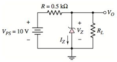
Problem 1.1EP: Calculate the intrinsic carrier concentration in gallium arsenide and germanium at T=300K . (Ans.... Problem 1.2EP: (a) Calculate the majority and minority carrier concentrations in silicon at T=300K for (i)... Problem 1.3EP: Consider ntype GaAs at T=300K doped to a concentration of Nd=21016cm3 . Assume mobility values of... Problem 1.4EP: Consider silicon at T=300K . Assume the hole concentration is given by p=1016ex/Lp(cm3) , where... Problem 1.1TYU: Determine the intrinsic carrier concentration in silicon, germanium, and GaAs at (a) T=400K and (b)... Problem 1.2TYU: (a) Consider silicon at T=300K . Assume that n=1350cm2/Vs and p=480cm2/Vs . Determine the... Problem 1.3TYU: Using the results of TYU1.2, determine the drift current density if an electric field of 4 V/cm is... Problem 1.4TYU: The electron and hole diffusion coefficients in silicon are Dn=35cm2/s and Dp=12.5cm2/s ,... Problem 1.5TYU: A sample of silicon at T=300K is doped to Nd=81015cm3 . (a) Calculate no and po . (b) If excess... Problem 1.5EP: (a) Calculate Vbi for a GaAs pn junction at T=300K for Na=1016cm3 and Nd=1017cm3 (b) Repeat part (a)... Problem 1.6EP: A silicon pn junction at T=300K is doped at Nd=1016cm3 and Na=1017cm3 . The junction capacitance is... Problem 1.7EP: (a) A silicon pn junction at T=300K has a reversesaturation current of IS=21014A . Determine the... Problem 1.6TYU: (a) Determine Vbi for a silicon pn junction at T=300K for Na=1015cm3 and Nd=51016cm3 . (b) Repeat... Problem 1.7TYU: A silicon pn junction diode at T=300K has a reversesaturation current of IS=1016A . (a) Determine... Problem 1.8TYU: Recall that the forwardbias diode voltage decreases approximately by 2mV/C for silicon diodes with a... Problem 1.8EP: Consider the circuit in Figure 1.28. Let VPS=4V , R=4k , and IS=1012A . Determine VD and ID , using... Problem 1.9EP: (a) Consider the circuit shown in Figure 1.28. Let VPS=8V and V=0.7V , Assume rf=0 . Calculate the... Problem 1.10EP: The resistor parameter in the circuit shown in Figure 1.28 is changed to R=20k . Using a PSpice... Problem 1.9TYU: Consider the diode and circuit in Exercise EX 1.8. Determine VD and ID , using the graphical... Problem 1.10TYU: Consider the circuit in Figure 1.28. Let R=4k and V=0.7V . Determine ID for (a) VPS=0.5V , (b)... Problem 1.11TYU: The power supply (input) voltage in the circuit of Figure 1.28 is VPS=10V and the diode cutin... Problem 1.11EP: (a) The circuit and diode parameters for the circuit shown in Figure 1.35(a) are VPS=8V , R=20k ,... Problem 1.12TYU: Determine the diffusion conductance of a pn junction diode at T=300K and biased at a current of 0.8... Problem 1.13TYU: Determine the smallsignal diffusion resistance of a pn junction diode at ID=10A , 100A , and 1 mA.... Problem 1.14TYU: The diffusion resistance of a pn junction diode at T=300K is determined to be rd=50 . What is the... Problem 1.12EP: A pn junction diode and a Schottky diode both have forwardbias currents of 1.2 mA. The... Problem 1.13EP: Consider the circuit shown in Figure 1.45. Determine the value of resistance R required to limit the... Problem 1.15TYU: Consider the circuit shown in Figure 1.46. The diode can be either a pn junction diode or a Schottky... Problem 1.16TYU: A Zener diode has an equivalent series resistance of 20 . If the voltage across the Zener diode is... Problem 1.17TYU: The resistor in the circuit shown in Figure 1.45 has a value of R=4k , the Zener diode breakdown... Problem 1RQ: Describe an intrinsic semiconductor material. What is meant by the intrinsic carrier concentration? Problem 2RQ: Describe the concept of an electron and a hole as charge carriers in the semiconductor material. Problem 3RQ: Describe an extrinsic semiconductor material. What is the electron concentration in terms of the... Problem 4RQ: Describe the concepts of drift current and diffusion current in a semiconductor material. Problem 5RQ: How is a pn junction formed? What is meant by a builtin potential barrier, and how is it formed? Problem 6RQ: How is a junction capacitance created in a reversebiased pn junction diode? Problem 7RQ: Write the ideal diode currentvoltage relationship. Describe the meaning of IS and VT . Problem 8RQ: Describe the iteration method of analysis and when it must be used to analyze a diode circuit. Problem 9RQ: Describe the piecewise linear model of a diode and why it is useful. What is the diode turnon... Problem 10RQ: Define a load line in a simple diode circuit. Problem 11RQ: Under what conditions is the smallsignal model of a diode used in the analysis of a diode circuit? Problem 12RQ: Describe the operation of a simple solar cell circuit. Problem 13RQ: How do the i characteristics of a Schottky barrier diode differ from those of a pn junction diode? Problem 14RQ: What characteristic of a Zener diode is used in the design of a Zener diode circuit? Problem 15RQ: Describe the characteristics of a photodiode and a photodiode circuit. Problem 1.1P: (a) Calculate the intrinsic carrier concentration in silicon at (i) T=250K and (ii) T=350K . (b)... Problem 1.2P: (a) The intrinsic carrier concentration in silicon is to be no larger than ni=1012cm3 . Determine... Problem 1.3P: Calculate the intrinsic carrier concentration in silicon and germanium at (a) T=100K , (b) T=300K ,... Problem 1.4P: (a) Find the concentration of electrons and holes in a sample of germanium that has a concentration... Problem 1.5P: Gallium arsenide is doped with acceptor impurity atoms at a concentration of 1016cm3 . (a) Find the... Problem 1.6P: Silicon is doped with 51016 arsenic atoms/cm3 . (a) Is the material n or ptype? (b) Calculate the... Problem 1.7P: (a) Calculate the concentration of electrons and holes in silicon that has a concentration of... Problem 1.8P: A silicon sample is fabricated such that the hole concentration is po=21017cm3 . (a) Should boron or... Problem 1.9P: The electron concentration in silicon at T=300K is no=51015cm3 , (a) Determine the hole... Problem 1.10P: (a) A silicon semiconductor material is to be designed such that the majority carrier electron... Problem 1.11P: (a) The applied electric field in ptype silicon is E=10V/cm . The semiconductor conductivity is... Problem 1.12P: A drift current density of 120A/cm2 is established in ntype silicon with an applied electric field... Problem 1.13P: An ntype silicon material has a resistivity of =0.65cm . (a) If the electron mobility is... Problem 1.14P: (a) The applied conductivity of a silicon material must be =1.5(cm)1 . If n=1000cm2/Vs and... Problem 1.15P: In GaAs, the mobilities are n=8500cm2/Vs and p=400cm2/Vs . (a) Determine the range in conductivity... Problem 1.16P: The electron and hole concentrations in a sample of silicon are shown in Figure P1.16. Assume the... Problem 1.17P: The hole concentration in silicon is given by p(x)=104+1015exp(x/Lp)x0 The value of Lp is 10m . The... Problem 1.18P: GaAs is doped to Na=1017cm3 . (a) Calculate no and po . (b) Excess electrons and holes are generated... Problem 1.19P: (a) Determine the builtin potential barrier Vbi in a silicon pn junction for (i) Nd=Na=51015cm3 ;... Problem 1.20P: Consider a silicon pn junction. The nregion is doped to a value of Nd=1016cm3 . The builtin... Problem 1.21P: The donor concentration in the nregion of a silicon pn junction is Nd=1016cm3 . Plot Vbi versus Na... Problem 1.22P: Consider a uniformly doped GaAs pn junction with doping concentrations of Nd=51018cm3 and... Problem 1.23P: The zerobiased junction capacitance of a silicon pn junction is Cjo=0.4pF . The doping... Problem 1.24P: The zerobias capacitance of a silicon pn junction diode is Cjo=0.02pF and the builtin potential is... Problem 1.25P: The doping concentrations in a silicon pn junction are Nd=51015cm3 and Na=1017cm3 . The zerobias... Problem 1.26P: (a) At what reversebias voltage does the reversebias current in a silicon pn junction diode reach 90... Problem 1.27P: (a) The reversesaturation current of a pn junction diode is IS=1011A . Determine the diode current... Problem 1.28P: (a) The reversesaturation current of a pn junction diode is IS=1011A . Determine the diode voltage... Problem 1.29P: A silicon pn junction diode has an emission coefficient of n=1 . The diode current is ID=1mA when... Problem 1.30P: Plot log10ID versus VD over the range 0.1VD0.7V for (a) IS=1012 and (b) IS=1014A . Problem 1.31P: (a) Consider a silicon pn junction diode operating in the forwardbias region. Determine the increase... Problem 1.32P: A pn junction diode has IS=2nA . (a) Determine the diode voltage if (i) ID=2A and (ii) ID=20A . (b)... Problem 1.33P: The reversebias saturation current for a set of diodes varies between 51014IS51012A . The diodes are... Problem 1.34P: A germanium pn junction has a diode current of ID=1.5mA when biased at VD=0.30V . What is the... Problem 1.35P: (a)The reversesaturation current of a gallium arsenide pn junction diode is IS=1022A . Determine the... Problem 1.36P: The reversesaturation current of a silicon pn junction diode at T=300K is IS=1012A . Determine the... Problem 1.37P: A silicon pn junction diode has an applied forwardbias voltage of 0.6 V. Determine the ratio of... Problem 1.38P: A pn junction diode is in series with a 1M resistor and a 2.8 V power supply. The reversesaturation... Problem 1.39P: Consider the diode circuit shown in Figure P1.39. The diode reversesaturation current is IS=1012A .... Problem 1.40P: The diode in the circuit shown in Figure P1.40 has a reversesaturation current of IS=51013A .... Problem 1.41P Problem 1.42P: (a) The reversesaturation current of each diode in the circuit shown in Figure P1.42 is IS=61014A .... Problem 1.43P: (a) Consider the circuit shown in Figure P1.40. The value of R1 is reduced to R1=10k and the cut-in... Problem 1.44P: Consider the circuit shown in Figure P1.44. Determine the diode current ID and diode voltage VD for... Problem 1.46P: The cutin voltage of the diode shown in the circuit in Figure P1.46 is V=0.7V . The diode is to... Problem 1.47P: Find I and VO in each circuit shown in Figure P1.47 if (i) V=0.7V and (ii) V=0.6V . Figure P1.47 Problem 1.48P: Repeat Problem 1.47 if the reversesaturation current for each diode isy IS=51014A . What is the... Problem 1.49P: (a) In the circuit Shown in Figure P1.49, find the diode voltage VD and the supply voltage V such... Problem 1.50P: Assume each diode in the circuit shown in Figure P1.50 has a cutin voltage of V=0.65V . (a) The... Problem 1.51P: (a) Consider a pn junction diode biased at IDQ=1mA . A sinusoidal volt age is superimposed on VDQ... Problem 1.52P: Determine the smallsignal diffusion resistancefor a diode biased at (a) (b) and (c) m:math... Problem 1.53P: The diode in the circuit shown in Figure P1.53 is biased with a constant current source I. A... Problem 1.54P: The forwardbias currents in a pn junction diode and a Schottky diode are 0.72 mA. The... Problem 1.55P: A pn junction diode and a Schottky diode have equal crosssectional areas and have forwardbias... Problem 1.56P: The reversesaturation currents of a Schottky diode and a pn junction diode are IS=5108A and 1012A ,... Problem 1.57P: Consider the Zener diode circuit shown in Figure P1.57. The Zener break down voltage is VZ=5.6V at... Problem 1.58P: (a) The Zener diode in Figure P1.57 is ideal with VZ=6.8V . Determine the maximum current and... Problem 1.59P: Consider the Zener diode circuit shown in Figure P1.57. The Zener diode voltage is VZ=6.8V at... Problem 1.60P: The Output current of a pn junction diode used as a solar cell can be given by ID=0.251014[exp( V D... Problem 1.61P: Using the currentvoltage characteristics of the solar cell described in Problem 1.60, plot ID versus... Problem 1.62P: (a) Using the currentvoltage characteristics of the solar cell described in problem 1.60, determine... Problem 1.63CSP: Use a computer simulation to generate the ideal currentvoltage characteristics of a diode from a... Problem 1.66CSP: Use a computer simulation to find the diode current, diode voltage, and output voltage for each... Problem D1.67DP: Design a diode circuit to produce the load line and Qpoint shown in Figure P1.67. Assume diode... Problem D1.68DP: Design a circuit to produce the characteristics shown in Figure P1.68, where iD is the diode current... Problem D1.69DP: Design a circuit to produce the characteristics shown in Figure P1.69, where O is the output voltage... Problem D1.70DP: Design a circuit to produce the characteristics shown in Figure P 1.70, where O is the output... format_list_bulleted


 Delmar's Standard Textbook Of ElectricityElectrical EngineeringISBN:9781337900348Author:Stephen L. HermanPublisher:Cengage Learning