Microelectronics: Circuit Analysis and Design
4th Edition
ISBN: 9780073380643
Author: Donald A. Neamen
Publisher: McGraw-Hill Companies, The
bartleby

Videos

Textbook Question
Book Icon
Chapter 7, Problem 7.10EP

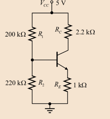
For the circuit in Figure 7.41(a), the parameters are, R 1 = 200 , R 2 = 220 R C = 2.2 , R C = 2.2 , R L = 4.7 , R E = 1 , r s = 100 , and V C C = 5 V . The transistor parameters are β o = 100 , V B E (on)=0 .7V , V A = , and C π = 1 pF . Consider the simplified hybrid− π model of the transistor. (a) Determine the midband current gain A i = I o / I i . (b) Find the Miller capacitance C M for (i) C μ = 0 and (ii) C μ = 0.08 pF . (c) Determine the upper 3dB frequency for
(i) C μ = 0 and (ii) C μ = 0.08 pF . (Ans. (a) A i = 30.24 ; (b) (i) C M = 0 , (ii) C M = 4.38 pF ; (c) f 3 d B = 60.2 MHz , (ii) f 3 d B = 11.2 MHz )

a.

Expert Solution
Check Mark
To determine

The midband current gain.

Answer to Problem 7.10EP

The value of mid-band current gain Ai is -30.24A/A.

Explanation of Solution

Given:

The parameters for the given circuit:

  R1=200kΩR2=220kΩRC=2.2kΩRL=4.7kΩRE=1kΩrS=100kΩVCC=5Vβo=100VBE( on)=0.7VVA=Cπ=1pF

Drawing the DC equivalent circuit for the given circuit:

  Microelectronics: Circuit Analysis and Design, Chapter 7, Problem 7.10EP , additional homework tip  1

Evaluating the Thevenin equivalent voltage at the base terminal:

  VTH=( R 2 R 1 + R 2 )VCC=( 220 200+220)(5)=2.62V

Evaluating the Thevenin equivalent resistance at the base terminal:

  RTH=R1𑨀R2=( R 1 R 2 R 1 + R 2 )=200×220200+220=104.76

Drawing the DC equivalent circuit as shown below:

  Microelectronics: Circuit Analysis and Design, Chapter 7, Problem 7.10EP , additional homework tip  2

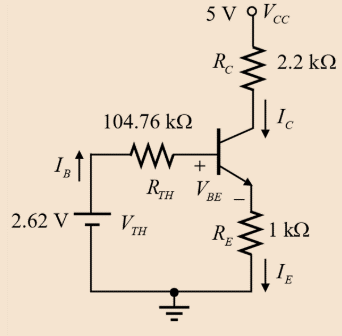
Evaluating the value of base current IB :

  IB=V THV BE( on )R TH+( β 0 +1)RE=2.620.7( 104.76× 10 3 )+( 100+1)( 1× 10 3 )=9.33×106=9.33μA

Evaluating the value of collector current IC :

  IC=β0IB=(100)(9.33× 10 6)=0.933mA

Evaluating the value of small signal parameters gm :

  gm=ICVT=0.933× 10 626× 10 3=35.88×103=35.88mA/V

Evaluating the value of small signal parameters rπ :

  rπ=βogm=10035.88× 10 3=2.78kΩ

Drawing the small-signal equivalent circuit for the mid band current gain:

  Microelectronics: Circuit Analysis and Design, Chapter 7, Problem 7.10EP , additional homework tip  3

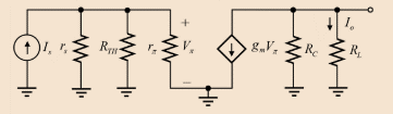
Applying the nodal analysis at the node Vπ :

  Vπrπ+VπR TH+Vπrs=IsVπ(1 r π +1 R TH +1 r s )=IsVπ=(rπ𑨀R TH𑨀rs)Is

Applying the current division rule at the output node:

  I0=RCRC+RL(gmVπ)I0=gmRCRC+RL(rπ𑨀R TH𑨀rs)IsI0Is=gmRCRC+RL(rπ𑨀R TH𑨀rs)

Evaluating the value of mid band current gain Ai :

  Ai=gmRCRC+RL(rπ𑨀R TH𑨀rs)=( 35.88× 10 3 )( 2.2× 10 3 )( 2.2× 10 3 )+( 4.7× 10 3 )(1 1 104.76× 10 3 + 1 2.786× 10 3 + 1 100× 10 3 )=( 35.88× 10 3 )( 2.2× 10 3 )( 2.642× 10 3 )( 6.9× 10 3 )=30.24A/A

Hence, the value of mid-band current gain Ai is -30.24A/A.

b.

Expert Solution
Check Mark
To determine

The Miller capacitance CM for the given values of the Cμ .

Answer to Problem 7.10EP

The Miller capacitances for the both cases are:

  (i)ForCμ=0CM=0(ii)For Cμ=0.08pFCM=4.38pF

Explanation of Solution

Given:

The parameters for the given circuit:

  R1=200kΩR2=220kΩRC=2.2kΩRL=4.7kΩRE=1kΩrS=100kΩVCC=5Vβo=100VBE( on)=0.7VVA=Cπ=1pF

The value of the capacitances are given as:

  (i)Cμ=0(ii)Cμ=0.08pF

( i ) The value of capacitance Cμ :

  Cμ=0

Evaluating the value of Miller capacitance for Cμ=0 .

  CM=Cμ[1+gm( R C𑨀 R L)]=(0)[1+gm( R C𑨀 R L)]=0

Hence, the value of Miller capacitance for Cμ=0 is CM=0 .

(ii)

The value of capacitance:

  Cμ=0.08pF

Evaluating the value of Miller capacitance for Cμ=0.08pF .

  CM=Cμ[1+gm( R C𑨀 R L)]=(0.08pF)[1+(35.88× 10 3)( 2.2× 10 3 )( 4.7× 10 3 )( 2.2× 10 3 )+( 4.7× 10 3 )]=(0.08pF)[1+(35.88× 10 3)(1.49855× 10 3)]=4.38pF

Hence, the value of the Miller capacitance for Cμ=0.08pF is CM=4.38pF .

c.

Expert Solution
Check Mark
To determine

The upper 3-dB frequency for the given values of the Cμ .

Answer to Problem 7.10EP

The 3-dB frequencies for the both cases are:

  (i)ForCμ=0f3dB=60.2MHz(ii)For Cμ=0.08pFf3dB=11.2MHz

Explanation of Solution

Given:

The parameters for the given circuit:

  R1=200kΩR2=220kΩRC=2.2kΩRL=4.7kΩRE=1kΩrS=100kΩVCC=5Vβo=100VBE( on)=0.7VVA=Cπ=1pF

The value of the capacitances are given as:

  (i)Cμ=0(ii)Cμ=0.08pF

(i)

The value of Miller capacitance for Cμ=0 :

Since, CM=0 for this case.

Evaluating the upper 3dB frequency for Cμ=0 :

  f3dB=12π( r s 𑨀 R TH 𑨀 r π )( C π + C M )=12π[( 1 1 104.76× 10 3 + 1 2.786× 10 3 + 1 100× 10 3 )]( 1× 10 12 +0)=12π( 2.642× 10 3 )( 1× 10 12 )=60.2MHz

Hence, the upper 3dB frequency for Cμ=0 is f3dB=60.2MHz

(ii)

The value of Miller capacitance for Cμ=0.08pF is

Since, CM=4.38pF for this case.

Evaluating the upper 3dB frequency for Cμ=0.08pF .

  f3dB=12π( r s 𑨀 R TH 𑨀 r π )( C π + C M )=12π[( 1 1 104.76× 10 3 + 1 2.786× 10 3 + 1 100× 10 3 )]( 1× 10 12 +4.38× 10 12 )=12π( 2.642× 10 3 )( 5.38× 10 12 )=11.2MHz

Hence, the upper 3dB frequency for Cμ=0.08pF is f3dB=11.2MHz .

Want to see more full solutions like this?

Subscribe now to access step-by-step solutions to millions of textbook problems written by subject matter experts!
Students have asked these similar questions
Answer as quickly as possible. I'll give upvote. Thank you. The circuit shown is a common source amplifier with a current mirror bias. It is given that the NMOS (M1) parameters are μoCox = 3mA/V2, VTH,n = 0.5V and λ = 0.02 and the PMOS (M2 and M3) parameters are μoCox = 1mA/V2 and VTH,p = −0.6V . The PMOS transistor M3 does not have channel length modulation while PMOS transistor M2 has λ = 0.02. It is also given that the dimensions of M2 and M3 have equal widths of 5µm and lengths of L2 = 3µm and L3 = 1.5µm, respectively. M1 has length of L1 = 1µm and width of W1 = 2µm. Find the gm and ro of transistor M1.
Question 7.15 Common gate configuration For the network of Fig. 7.92, determine:a. IDQ and VGSQ.b. VDS and VS.
Answer ASAP. I'll upvote. Thank you. Given: The circuit shown is a common source amplifier with a current mirror bias. It is given that the NMOS (M1) parameters are μoCox = 3mA/V2, VTH,n = 0.5V and λ = 0.02 and the PMOS (M2 and M3) parameters are μoCox = 1mA/V2 and VTH,p = −0.6V . The PMOS transistor M3 does not have channel length modulation while PMOS transistor M2 has λ = 0.02. It is also given that the dimensions of M2 and M3 have equal widths of 5µm and lengths of L2 = 3µm and L3 = 1.5µm, respectively. M1 has length of L1 = 1µm and width of W1 = 2µm. Sketch the small signal model of transistor M3 (Hint: Is there any small signal in any terminal ofM3? If yes, then where is it? If no, then what happens to the small signal model?).

Chapter 7 Solutions

Microelectronics: Circuit Analysis and Design

Ch. 7 - The commonemitter circuit shown in Figure 7.34...Ch. 7 - A bipolar transistor has parameters o=120 ,...Ch. 7 - Prob. 7.9EPCh. 7 - For the circuit in Figure 7.41(a), the parameters...Ch. 7 - A bipolar transistor is biased at ICQ=120A and its...Ch. 7 - For the transistor described in Example 7.9 and...Ch. 7 - The parameters of a bipolar transistor are: o=150...Ch. 7 - The parameters of an nchannel MOSFET are...Ch. 7 - For the circuit in Figure 7.55, the transistor...Ch. 7 - An nchannel MOSFET has parameters Kn=0.4mA/V2 ,...Ch. 7 - An nchannel MOSFET has a unitygain bandwidth of...Ch. 7 - For a MOSFET, assume that gm=1.2mA/V . The basic...Ch. 7 - The transistor in the circuit in Figure 7.60 has...Ch. 7 - Consider the commonbase circuit in Figure 7.64....Ch. 7 - The cascode circuit in Figure 7.65 has parameters...Ch. 7 - Prob. 7.12TYUCh. 7 - For the circuit in Figure 7.72, the transistor...Ch. 7 - Describe the general frequency response of an...Ch. 7 - Describe the general characteristics of the...Ch. 7 - Describe what is meant by a system transfer...Ch. 7 - What is the criterion that defines a corner, or...Ch. 7 - Describe what is meant by the phase of the...Ch. 7 - Describe the time constant technique for...Ch. 7 - Describe the general frequency response of a...Ch. 7 - Sketch the expanded hybrid model of the BJT.Ch. 7 - Prob. 9RQCh. 7 - Prob. 10RQCh. 7 - Prob. 11RQCh. 7 - Sketch the expanded smallsignal equivalent circuit...Ch. 7 - Define the cutoff frequency for a MOSFET.Ch. 7 - Prob. 14RQCh. 7 - Why is there not a Miller effect in a commonbase...Ch. 7 - Describe the configuration of a cascode amplifier.Ch. 7 - Why is the bandwidth of a cascode amplifier...Ch. 7 - Why is the bandwidth of the emitterfollower...Ch. 7 - Prob. 7.1PCh. 7 - Prob. 7.2PCh. 7 - Consider the circuit in Figure P7.3. (a) Derive...Ch. 7 - Consider the circuit in Figure P7.4 with a signal...Ch. 7 - Consider the circuit shown in Figure P7.5. (a)...Ch. 7 - A voltage transfer function is given by...Ch. 7 - Sketch the Bode magnitude plots for the following...Ch. 7 - (a) Determine the transfer function corresponding...Ch. 7 - Consider the circuit shown in Figure 7.15 with...Ch. 7 - For the circuit shown in Figure P7.12, the...Ch. 7 - The circuit shown in Figure 7.10 has parameters...Ch. 7 - The transistor shown in Figure P7.14 has...Ch. 7 - Consider the circuit shown in Figure P7.15. The...Ch. 7 - The transistor in the circuit shown in Figure...Ch. 7 - For the common-emitter circuit in Figure P7.17,...Ch. 7 - The transistor in the circuit in Figure P7.20 has...Ch. 7 - For the circuit in Figure P7.21, the transistor...Ch. 7 - (a) For the circuit shown in Figure P7.22, write...Ch. 7 - Consider the circuit shown in Figure P7.23. (a)...Ch. 7 - The parameters of the transistor in the circuit in...Ch. 7 - A capacitor is placed in parallel with RL in the...Ch. 7 - The parameters of the transistor in the circuit in...Ch. 7 - Prob. D7.27PCh. 7 - The circuit in Figure P7.28 is a simple output...Ch. 7 - Reconsider the circuit in Figure P728. The...Ch. 7 - Consider the circuit shown in Figure P7.32. The...Ch. 7 - The commonemitter circuit in Figure P7.35 has an...Ch. 7 - Consider the commonbase circuit in Figure 7.33 in...Ch. 7 - Prob. 7.39PCh. 7 - The parameters of the transistor in the circuit in...Ch. 7 - In the commonsource amplifier in Figure 7.25(a) in...Ch. 7 - A bipolar transistor has fT=4GHz , o=120 , and...Ch. 7 - A highfrequency bipolar transistor is biased at...Ch. 7 - (a) The frequency fT of a bipolar transistor is...Ch. 7 - The circuit in Figure P7.48 is a hybrid ...Ch. 7 - Consider the circuit in Figure P7.49. Calculate...Ch. 7 - A common-emitter equivalent circuit is shown in...Ch. 7 - For the common-emitter circuit in Figure 7.41(a)...Ch. 7 - For the commonemitter circuit in Figure P7.52,...Ch. 7 - Consider the circuit in Figure P7.52. The resistor...Ch. 7 - The parameters of the circuit shown in Figure...Ch. 7 - The parameters of an nchannel MOSFET are kn=80A/V2...Ch. 7 - Find fT for a MOSFET biased at IDQ=120A and...Ch. 7 - Fill in the missing parameter values in the...Ch. 7 - (a) An nchannel MOSFET has an electron mobility of...Ch. 7 - A commonsource equivalent circuit is shown in...Ch. 7 - Prob. 7.60PCh. 7 - The parameters of an ideal nchannel MOSFET are...Ch. 7 - Figure P7.62 shows the highfrequency equivalent...Ch. 7 - For the FET circuit in Figure P7.63, the...Ch. 7 - The midband voltage gain of a commonsource MOSFET...Ch. 7 - Prob. 7.65PCh. 7 - Prob. 7.67PCh. 7 - The bias voltages of the circuit shown in Figure...Ch. 7 - For the PMOS commonsource circuit shown in Figure...Ch. 7 - In the commonbase circuit shown in Figure P7.70,...Ch. 7 - Repeat Problem 7.70 for the commonbase circuit in...Ch. 7 - In the commongate circuit in Figure P7.72, the...
Knowledge Booster
Background pattern image
Electrical Engineering
Learn more about
Need a deep-dive on the concept behind this application? Look no further. Learn more about this topic, electrical-engineering and related others by exploring similar questions and additional content below.
Similar questions
SEE MORE QUESTIONS
Recommended textbooks for you
Text book image
Introductory Circuit Analysis (13th Edition)
Electrical Engineering
ISBN:9780133923605
Author:Robert L. Boylestad
Publisher:PEARSON
Text book image
Delmar's Standard Textbook Of Electricity
Electrical Engineering
ISBN:9781337900348
Author:Stephen L. Herman
Publisher:Cengage Learning
Text book image
Programmable Logic Controllers
Electrical Engineering
ISBN:9780073373843
Author:Frank D. Petruzella
Publisher:McGraw-Hill Education
Text book image
Fundamentals of Electric Circuits
Electrical Engineering
ISBN:9780078028229
Author:Charles K Alexander, Matthew Sadiku
Publisher:McGraw-Hill Education
Text book image
Electric Circuits. (11th Edition)
Electrical Engineering
ISBN:9780134746968
Author:James W. Nilsson, Susan Riedel
Publisher:PEARSON
Text book image
Engineering Electromagnetics
Electrical Engineering
ISBN:9780078028151
Author:Hayt, William H. (william Hart), Jr, BUCK, John A.
Publisher:Mcgraw-hill Education,
Diode Logic Gates - OR, NOR, AND, & NAND; Author: The Organic Chemistry Tutor;https://www.youtube.com/watch?v=9lqwSaIDm2g;License: Standard Youtube License