
Videos
In the common−source amplifier in Figure 7.25(a) in the text, a source bypass capacitor is to be added between the source terminal and ground potential. The circuit parameters are
a.
To derive: The small signal voltage gain expression.
Answer to Problem 7.41P
The expression for small signal voltage gain:
Explanation of Solution
Given:
The circuit parameter is given as:
The transistor parameter are given as:
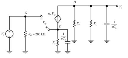
Drawing the small signal model of the circuit with the source bypass capacitor:
Applying the Ohm’s law to the drain terminal:
Evaluating the input voltage
Evaluating the ratio of output voltage to the input voltage:
Therefore, the expression for small signal voltage gain:
b.
The expression for the time constant associated with the upper 3dB frequency.
Answer to Problem 7.41P
The expression for the time constant associated with the upper 3 Db frequency is:
Explanation of Solution
Given:
The circuit parameter is given as:
The transistor parameter are given as:
The expression for time constant
Here, the expression for the time constant associated with the upper 3 Db frequency is:
c.
The time constant, upper 3 dB frequency and the small signal midband voltage gain.
Answer to Problem 7.41P
The small signal mid-band voltage gain is -4.7.
Explanation of Solution
Given:
The circuit parameter is given as:
The transistor parameter are given as:
The equation for the time constant is given as:
Substituting the known values in the above equation:
Hence, the value of time constant,
Now, evaluating the upper
Substitute
Hence, the value of upper
Applying the Kirchhoff s voltage law to the outer loop:
Substituting the known values:
Evaluating the value of current
Substituting the known values:
Evaluating the transconductance
Substituting the known values in the above equation:
Since, the voltage gain is given as:
Evaluating the mid-band voltage gain
Substituting the known values in the above equation:
Hence, the small signal mid-band voltage gain is -4.7.
Want to see more full solutions like this?
Chapter 7 Solutions
Microelectronics: Circuit Analysis and Design


- A bipolar transistor is operating with vBE =+0.7 V and vBC = +0.3 V. By the strict definitionsgiven in the chapter on bipolar transistors, this transistoris operating in the saturation region. Use thetransport equations to demonstrate that it actuallybehaves as if it is still in the forward-active region.Discuss this result. (You may use IS = 10−15 A,αF = 0.98, and αR = 0.2.)arrow_forwardDesign a VCO circuit that will produce a square wave output at 2.6 kHz.arrow_forwardA 5-V, 10-MHz oscillator have a rise/falltime of 10ns and a 50% duty cycle is applied to a gate. Determine the value of the capacitance such that the 5th harmonic is reduced by 20 dB in the gate voltage Vg(t).arrow_forward
- Most of the following statements about integrated circuits arecorrect, but one is not. Which statement is NOT true? Select one: a. Transistors are constructed in a small area of an integrated circuit,and are connected to other transistors by wires that are embedded inthe integrated circuit b. Wires that carry signals may be embedded in a substrate without a shortcircuit because a short circuit would require a signal to cross areverse biased junction c. Each transistor on an integrated circuit is manufactured individually,one at a time d. An integrated circuit contains several layersarrow_forwardIf the collector supply voltage is increased to 15 V in Fig. 7-30b, what is the collector-emitter voltage for VBB = 1.8 V?arrow_forwardIs my understanding about the plot of the input and output correct? In the given circuit, the capacitor will charge when the transistor is off and it will discharge through the transitor when the transistor is on. If the time constant is large(value of capacitor is increased), the capacitor charges slowly and will not reach its max value because the time the transistor is off will be shorter than the charging time?arrow_forward
- A Hartley Oscillator circuit having two individual inductors of 0.5mH each, are designed toresonate in parallel with a variable capacitor that can be adjusted between 100pF and 500pF.Determine the upper and lower frequencies of oscillation and also the Hartley oscillatorsbandwidth.arrow_forwardTrying to solve this MOSFET question but not sure how.(Given Answer:a) Av = -gm (ro|| RD)b)Av = -30.7 Ri = 20 kohm Ro = 7.67 kohm)arrow_forwardDetermine the DC bias values using DC equivalent circuits (in order of VE, VB, VC)arrow_forward
- A 5 V battery, a capacitor with a capacity of 15 mkF, and a resistance of 10 kOhm are connected in series in the electrical circuit. The relaxation time in such a chain is equal to?arrow_forwardAnswer ASAP. I'll upvote. Thank you. Given: The circuit shown is a common source amplifier with a current mirror bias. It is given that the NMOS (M1) parameters are μoCox = 3mA/V2, VTH,n = 0.5V and λ = 0.02 and the PMOS (M2 and M3) parameters are μoCox = 1mA/V2 and VTH,p = −0.6V . The PMOS transistor M3 does not have channel length modulation while PMOS transistor M2 has λ = 0.02. It is also given that the dimensions of M2 and M3 have equal widths of 5µm and lengths of L2 = 3µm and L3 = 1.5µm, respectively. M1 has length of L1 = 1µm and width of W1 = 2µm. Sketch the small signal model of transistor M3 (Hint: Is there any small signal in any terminal ofM3? If yes, then where is it? If no, then what happens to the small signal model?).arrow_forwarddescribe the working principle OF MOS (need only handwritten solution .otherwise downvote.)arrow_forward
 Introductory Circuit Analysis (13th Edition)Electrical EngineeringISBN:9780133923605Author:Robert L. BoylestadPublisher:PEARSON
 Delmar's Standard Textbook Of ElectricityElectrical EngineeringISBN:9781337900348Author:Stephen L. HermanPublisher:Cengage Learning
 Programmable Logic ControllersElectrical EngineeringISBN:9780073373843Author:Frank D. PetruzellaPublisher:McGraw-Hill Education
 Fundamentals of Electric CircuitsElectrical EngineeringISBN:9780078028229Author:Charles K Alexander, Matthew SadikuPublisher:McGraw-Hill Education
 Electric Circuits. (11th Edition)Electrical EngineeringISBN:9780134746968Author:James W. Nilsson, Susan RiedelPublisher:PEARSON
 Engineering ElectromagneticsElectrical EngineeringISBN:9780078028151Author:Hayt, William H. (william Hart), Jr, BUCK, John A.Publisher:Mcgraw-hill Education,