
Videos
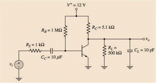
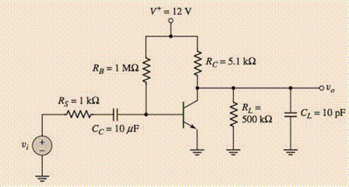
The parameters of the transistor in the circuit in Figure P7.40 are
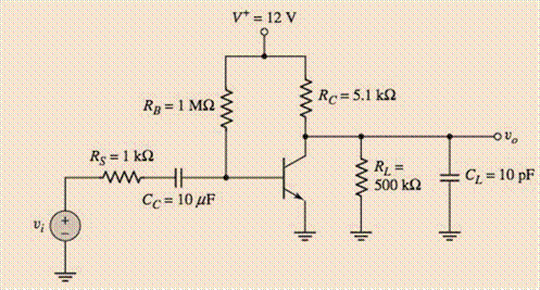
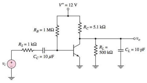 Figure P7.40
a.
To draw: Three equivalent circuits that represent the amplifier in the low frequency range, mid-band range and the high frequency range.
Answer to Problem 7.40P
Three equivalent circuits that represent the amplifier in the low frequency range, mid-band range and the high frequency range are shown in Figure 1, 2 and 3 respectively.
Explanation of Solution
Given:
The diagram is given as:
Calculation:
Calculate the value of current
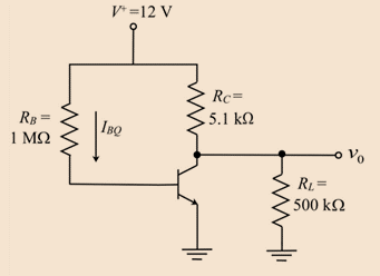
Applying Kirchhoff s voltage law in the above loop:
Here,
Substituting
The quiescent collector current
Here,
Substituting
Evaluating the resistance
Here,
Evaluating the transconductance
Substituting
Figure 2 shows the low −frequency small signal transistor with the output resistance
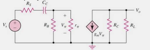
Figure 1
In the mid-frequency range, the coupling and bypass capacitors are short-circuited and the load capacitors are open-circuited.
It shows the mid-frequency small signal transistor with the output resistance
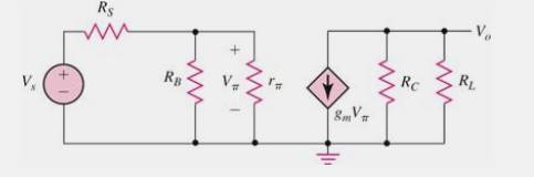
Figure 2
In the high-frequency range, the coupling and bypass capacitors are short-circuited and the load capacitors are included.
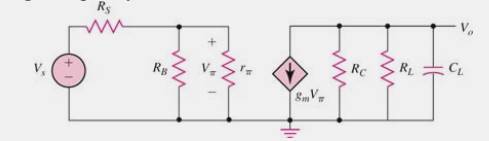
Figure 3
Hence, the three equivalent circuits that represent the amplifier in the low-frequency range, mid-band range, and high-frequency range are plotted.
b.
To sketch: The bode magnitude plot.
Answer to Problem 7.40P
The sketch of bode magnitude plot is shown in Figure 4.
Explanation of Solution
Given:
The diagram is given as:
Calculation:
Consider the values, calculated in part (a).
The effect of the coupling capacitor
The figure shows the bode plot for the circuit having a combination of a coupling capacitor and load capacitor:
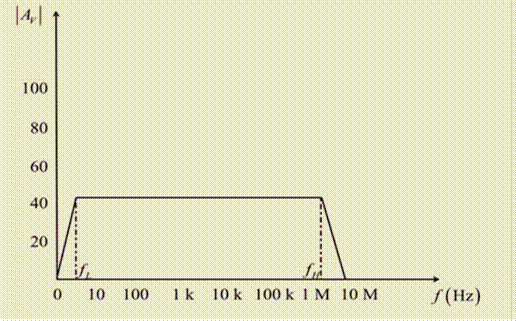
Figure 4
Hence, the bode magnitude plot is sketched.
c.
The values of the
Answer to Problem 7.40P
The values are:
Explanation of Solution
Given:
The diagram is given as:
Calculation:
Evaluating the midband gain by short-circuiting the coupling and bypass capacitors and open-circuiting the load capacitors.
Substituting the values,
Evaluating the gain in dB:
Substituting
Hence, the value of gain
Evaluating the equivalent resistance
Substituting
Evaluating the time constant
Substituting
Evaluating the equivalent resistance
Substituting
Evaluating the time constant
Substituting
Evaluate the lower corner frequency
Substituting
Evaluated the upper corner frequency:
Substitute
Want to see more full solutions like this?
Chapter 7 Solutions
Microelectronics: Circuit Analysis and Design
Additional Engineering Textbook Solutions
Electronics Fundamentals: Circuits, Devices & Applications
ANALYSIS+DESIGN OF LINEAR CIRCUITS(LL)
Fundamentals of Applied Electromagnetics (7th Edition)
Engineering Electromagnetics
Loose Leaf for Engineering Circuit Analysis Format: Loose-leaf
Programmable Logic Controllers


- For a mosfet amplifier circuit, how can I choose an input and output capacitor with poles at 10Hz and 100Hz? Where RC = 1/w.arrow_forwardWhat is the coherent bandwidth equation?arrow_forwardWhat are the advantages and disadvantages of single-sideband transmission? Briefly describe each.arrow_forward
- How many channels are available in the 2.4 GHz band? List all the channels. What is the channelbandwidth?arrow_forwardExlapin any one method of suppression of unwanted sideband in detail. Neat answer sir!arrow_forwardWhy is having a certain bandwidth so crucial? Please provide more details.arrow_forward
- The SNRi of an FM transmitter is determined to be 24.093dBV. Solve for the peak frequency deviation caused by the noise if the transmitter sensitivity is determined to be 368.903Hz/V, and a modulating signal of 13.926V and the modulating index is kept at 4arrow_forwardDescribe the general characteristics of the equivalent circuits that apply to the low frequency,midband,and high frequency ranges.arrow_forwarda) Sketch the spectrum of g(t)?b) Sketch the spectrum at point (a) of the conversion system?c) What should the parameter w0 be relative to wc?d) What should be the value of passband gain A?arrow_forward
- 2 (AM) A 10 V amplitude sinusoidal signal is used as a modulating signal to generate an AM signal with modulation index 0.8. What is the amplitude of the carrier? What is the power of the side bands? What is the efficiency of the modulated signal?arrow_forwardWhat are the relative amplitudes of the fourth pair of sidebands for an FM signal with a deviation ratio of 8?arrow_forwardBriefly explain what it is Single Sideband Modulationarrow_forward
 Introductory Circuit Analysis (13th Edition)Electrical EngineeringISBN:9780133923605Author:Robert L. BoylestadPublisher:PEARSON
 Delmar's Standard Textbook Of ElectricityElectrical EngineeringISBN:9781337900348Author:Stephen L. HermanPublisher:Cengage Learning
 Programmable Logic ControllersElectrical EngineeringISBN:9780073373843Author:Frank D. PetruzellaPublisher:McGraw-Hill Education
 Fundamentals of Electric CircuitsElectrical EngineeringISBN:9780078028229Author:Charles K Alexander, Matthew SadikuPublisher:McGraw-Hill Education
 Electric Circuits. (11th Edition)Electrical EngineeringISBN:9780134746968Author:James W. Nilsson, Susan RiedelPublisher:PEARSON
 Engineering ElectromagneticsElectrical EngineeringISBN:9780078028151Author:Hayt, William H. (william Hart), Jr, BUCK, John A.Publisher:Mcgraw-hill Education,