
Concept explainers
(a)
The base and the collector current in each of the transistor. Also, the power dissipation in the gate.
(a)
Answer to Problem 17.12EP
The currents in the transistors are,
Explanation of Solution
Calculation:
The given diagram is shown in Figure 1
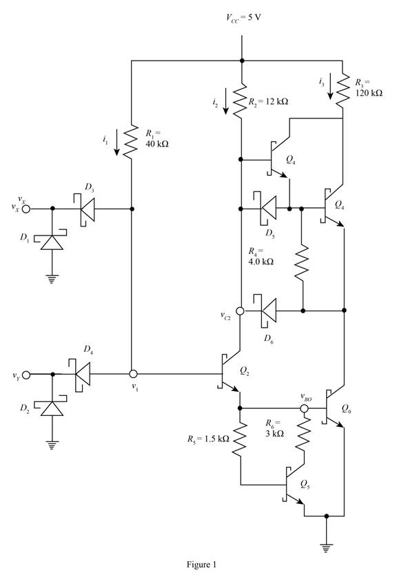
The expression to determine the value of the voltage
Substitute
The expression to determine the value of the current
Substitute
The conversion from
The conversion from
The second transistor and the output transistor are in cut off region and the current in the circuit are given by,
The expression for the value of the collector current and the base current of the output transistor is given by,
The expression for the base and the collector current of the third and the fourth transistor are given by,
The expression for the power dissipated in the circuit is given by,
Substitute
Conclusion:
Therefore, the currents in the transistors are,
(b)
The base and the collector current in each of the transistor. Also, the power dissipation in the gate.
(b)
Answer to Problem 17.12EP
The currents in the transistors are,
Explanation of Solution
Calculation:
The expression to determine the value of the voltage
Substitute
The expression for the voltage
Substitute
The expression to determine the value of the current
Substitute
The expression to determine the value of the current
Substitute
The conversion from
The conversion from
The expression for the base current of the second transistor is given by,
Substitute
The expression for the collector current of the second transistor is given by,
Substitute
The fifth transistor is in the cut off region and the current in the circuit are given by,
The expression for the value of the collector current of output transistor is given by,
Substitute
The expression for the base and the collector current of the third and the fourth transistor are given by,
The expression for the power dissipated in the circuit is given by,
Substitute
The conversion from
The conversion from
Conclusion:
Therefore, the currents in the transistors are,
Want to see more full solutions like this?
Chapter 17 Solutions
Microelectronics: Circuit Analysis and Design


- State the advantages and disadvantages of theDSB_LCarrow_forwardEstimate iB and iC of the Schottky transistor shown if the external collector terminal isopen. Assume the forward voltage of the Schottkydiode is 0.45 V.arrow_forward15. How many OC signals are used in a SONET network with a 622.08 Mbps line rate?A. 8064B. 4C. 12D. 8arrow_forward
- Draw the schematic of a three-input NAND gate. What are the W/L ratios for thetransistors based?arrow_forwardIn the figure below, an x(t) signal varying between +- 1.6 V is split into 8 quanta levels and converted to a digital signal. being converted. a) Calculate the quantization gap voltage (step)? b) Draw the PAM, PCM and ASK outputs in this conversion process? c) Calculate bit transmission rate if sampling pulse frequency ?? = 2kHz.arrow_forwardSuggest another FSK modulation circuit and explain its operation briefly.arrow_forward
- Find the BER of a 64-QAM system with SNR=10 dB. NOTE: Use Q-function table as needed.arrow_forwardDraw (a) the multiple-level NOR circuit for the following expression: CD(B+C)A+(BC′+DE′), and (b) repeat (a) for a NAND circuit.arrow_forwardThe number of bits per sample in a PCM system has SNqR=45 dB is?arrow_forward
- 4/ For a QPSK modulator with a 10 Mbps transmission rate and a carrier frequency 70 kHz. Consider a high cosine pulse with r = 0.5. (1 A/ Determine the minimum transmission bandwidth B/ Determine the wide width of a BPSK modulator with the same data transmission rate and the same type of pulse.arrow_forwardFor a QPSK waveform, with the following input bit sequence 100010101101, an input rate equal to 20 Mbps: Draw the modulated waveform, state assumption used. Determine the minimum bandwidth requiredarrow_forward7. The advantage of a differential phase-shift keying (DPSK) system is that_____________ is (are) not required.A. carrier synchronizerB. voltage-controlled oscillatorsC. upper and lower sidebandsD. carrier recovery circuitryarrow_forward
 Introductory Circuit Analysis (13th Edition)Electrical EngineeringISBN:9780133923605Author:Robert L. BoylestadPublisher:PEARSON
 Delmar's Standard Textbook Of ElectricityElectrical EngineeringISBN:9781337900348Author:Stephen L. HermanPublisher:Cengage Learning
 Programmable Logic ControllersElectrical EngineeringISBN:9780073373843Author:Frank D. PetruzellaPublisher:McGraw-Hill Education
 Fundamentals of Electric CircuitsElectrical EngineeringISBN:9780078028229Author:Charles K Alexander, Matthew SadikuPublisher:McGraw-Hill Education
 Electric Circuits. (11th Edition)Electrical EngineeringISBN:9780134746968Author:James W. Nilsson, Susan RiedelPublisher:PEARSON
 Engineering ElectromagneticsElectrical EngineeringISBN:9780078028151Author:Hayt, William H. (william Hart), Jr, BUCK, John A.Publisher:Mcgraw-hill Education,