
Videos
For the differential amplifier circuit ¡n Figure P17.1, neglect the base currents. (a) Determine
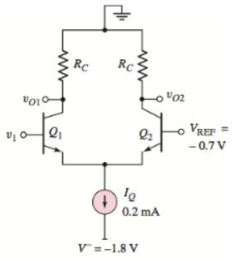
Figure P17.1
Want to see the full answer?
Check out a sample textbook solution
Chapter 17 Solutions
Microelectronics: Circuit Analysis and Design


- AC analysis: The signal source is ??(?)=5sin?? mV. The transistor parameters are β = 120 and VA = ∞. (a) (i) Design the circuit such that ??? = 0.25 mA and ???? = 3 V. (ii) Find the small-signal voltage gain ??=????⁄. (iii) Find ??(?). (b) Repeat part (a) for RS = 0.arrow_forward2. The SNRo of a receiver is determined to be 35.937dB. Determine the SNRi in dB, if the modulation index is kept at 2 and the modulating signal is determined to have a peak voltage of 12.452. It is also noted that the system's sensitivity to changes in frequency is 200.718Hz/V. This modulator is using the maximum frequency deviation.arrow_forwarddesign a butterworth 1st order low pass filter . explain and calculate its Voarrow_forward
- Develop the truth table and constellation diagram of QPSK using I -channel reference cos wct and 90 degrees phase shift for IQ inputs 00 and 10. Draw the analog output waveform of the given inputsarrow_forwardExplain the output response of a second order system.arrow_forwardBriefly explain the Nyquist theorem in the context of digital sampling.arrow_forward
- 3/ A Digital Analog Converter of 12 Bits of Precision is available A/ Determine the signal to the system's peak noise ratio B/ If the signal is sampled at 44 kHz. What is the bits rate generated by the system? C/ Determine the required bandwidth if I wanted to transmit this data with a modulator 16-QAM.arrow_forwardIdentify the process of dividing a voltage range into discrete increments, each of which is represented by a binary number. Clipping Quantizing Modulating Samplingarrow_forwardWhat is the term used to express the ability of a measuring system to maintain its standard performance? a) Zero Reliabilityb) Stabilitye) Sensitivityd) Linearityarrow_forward
- For the LC Oscillator shown a. Calculate the minimum amplifier gain needed to sustain oscillation b. is the amplifier an inverting or non inverting? whyarrow_forwardThe Type K thermocouple has a sensitivity of about 41 micro-Volts/℃, i.e. for each degree difference in the junction temperature, the output changes by 41 micro-Volts. Among 8-bit, 12-bit, 16-bit, 32-bit and 64-bit ADC, which is the most appropriate for measuring human body temperature to 4th decimal place (appropriate = accurate yet cost-effective), if the ADC range is 10 V?arrow_forwardFor a PCM system with the following parameters, Parameters: (i) Maximum analog input frequency = 5 kHz; (ii) Maximum decoded voltage at the receiver = ±5.01 V; (iii) Minimum dynamic range = 54 dB. (Use 2 decimal places) a) What is the coding efficiency in % b) What is the resolution in V? c) Determine the maximum quantization error in V.arrow_forward
 Introductory Circuit Analysis (13th Edition)Electrical EngineeringISBN:9780133923605Author:Robert L. BoylestadPublisher:PEARSON
 Delmar's Standard Textbook Of ElectricityElectrical EngineeringISBN:9781337900348Author:Stephen L. HermanPublisher:Cengage Learning
 Programmable Logic ControllersElectrical EngineeringISBN:9780073373843Author:Frank D. PetruzellaPublisher:McGraw-Hill Education
 Fundamentals of Electric CircuitsElectrical EngineeringISBN:9780078028229Author:Charles K Alexander, Matthew SadikuPublisher:McGraw-Hill Education
 Electric Circuits. (11th Edition)Electrical EngineeringISBN:9780134746968Author:James W. Nilsson, Susan RiedelPublisher:PEARSON
 Engineering ElectromagneticsElectrical EngineeringISBN:9780078028151Author:Hayt, William H. (william Hart), Jr, BUCK, John A.Publisher:Mcgraw-hill Education,