
Concept explainers
Videos
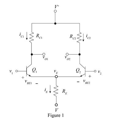
Consider the differential amplifier circuit in Figure 17.1 biased at
(a)
The design parameters of the circuit for the given values.
Answer to Problem 17.1EP
The value of the resistances to design the circuit are for
Explanation of Solution
Calculation:
The given circuit is shown in Figure 1.
The expression for the voltage at the emitter terminals is given by,
Substitute
The expression to determine the value of the current
Substitute
The expression to determine the value of the collector current of the first transistor is given by,
Substitute
The expression for the value of the collector current of the second transistor is given by,
Substitute
The expression for the value of the voltage
Substitute
Conclusion:
Therefore, the value of the resistances to design the circuit are for
(b)
The value of the current
Answer to Problem 17.1EP
The value of the current and the voltage for the value of the input voltage of
Explanation of Solution
Calculation:
The expression for the voltage at the emitter terminals is given by,
Substitute
The expression to determine the value of the current
Substitute
The expression to determine the value of the collector current of the first transistor is given by,
Substitute
The expression for the value of the collector current of the second transistor is given by,
The expression for the value of the voltage
Substitute
The expression for the value of the voltage
Substitute
The expression for the voltage at the emitter terminals is given by,
Substitute
The expression to determine the value of the current
Substitute
The expression to determine the value of the collector current of the first transistor is given by,
The expression for the value of the collector current of the second transistor is given by,
Substitute
The expression for the value of the voltage
Substitute
The expression for the value of the voltage
Substitute
Conclusion:
Therefore, the value of the current and the voltage for the value of the input voltage of
(c)
The value of the power dissipated in the circuit for the different value of the input voltage.
Answer to Problem 17.1EP
The value of the power consumed in the circuit for the input voltage of
Explanation of Solution
Calculation:
The expression for the value of the power dissipated in the circuit.
Substitute
Substitute
Conclusion:
Therefore, the value of the power consumed in the circuit for the input voltage of
Want to see more full solutions like this?
Chapter 17 Solutions
Microelectronics: Circuit Analysis and Design


- Estimate iB and iC of the Schottky transistor shown if the external collector terminal isopen. Assume the forward voltage of the Schottkydiode is 0.45 V.arrow_forwardIV (a) If R = 25 Kohm and C = 12 uF, find the frequency of the astable multivibrator using NAND gate? Draw the diagram and its output waveform for Vcc = + 15 V. (b) If C=9nF, the frequency F=72KHz of the Monostable multivibrator using NAND gate . Find the value of resistance ?arrow_forwardConsider a CE circuit, where trans-conductance is 50mΩ-1, diffusion capacitance is 100 pF, transition capacitance is 3 pF. IB = 20μA. Given base emitter dynamic resistance, rbe = 1000 Ω, input VI is 20*sin(107t). What is the short circuit current gain?arrow_forward
- 2. The SNRo of a receiver is determined to be 35.937dB. Determine the SNRi in dB, if the modulation index is kept at 2 and the modulating signal is determined to have a peak voltage of 12.452. It is also noted that the system's sensitivity to changes in frequency is 200.718Hz/V. This modulator is using the maximum frequency deviation.arrow_forwardDraw and show the BFSK modulation waveform for the given binary data sequence “1,0,0,1”, and also draw its BFSK constellation diagram.arrow_forwardDraw the schematic of a three-input NAND gate. What are the W/L ratios for thetransistors based?arrow_forward
- For the circuit shown, let Vcc = 3.3V, RE = 500 Ω, RC = 4 kΩ, R1= 85 kΩ, R2 = 35 k Ω, and β = 150 Using approximation, determine the Q-point parameters: IBQ, ICQ, and VCEQ. Indicate the exact numerical values, following the given unit.arrow_forward(a) For the MOSFET figure, let VDD = 15V, R1 = 4.7 MΩ, R2 = 2.2 MΩ, RS = 1kΩ, RD = 4.2kΩ, Vt = 2V, and k = 0.5 mA/V2. Find VGS, ID, and VDS. (NOTE: use Wolfram Alpha Equation Solver.) (b) Repeat with same parameters, except RS = 0.arrow_forwardAC analysis: The signal source is ??(?)=5sin?? mV. The transistor parameters are β = 120 and VA = ∞. (a) (i) Design the circuit such that ??? = 0.25 mA and ???? = 3 V. (ii) Find the small-signal voltage gain ??=????⁄. (iii) Find ??(?). (b) Repeat part (a) for RS = 0.arrow_forward
- For the transistor , IS = 6×10⁻¹⁶ μA,αF = 0.985, and αR = 0.25. (a) What type oftransistor is in this circuit? (b) Label the collector, base, and emitter terminals of the transistor.(c) Label the emitter-base and collector-base voltages, and label the normal direction for IE , IC, andIB. (d) Write the simplified form of the transportmodel equations that apply to this particular circuitconfiguration. Write an expression for IE /IC. Writean expression for IE /IB. (e) Find the values of IE ,IC, IB, βF , βR, VE B, and VC B.arrow_forwardProblem: Fx=(AB+CD+EF+G)' a. Draw its equivalent transistor circuit. b. Determine if the function has an Euler's path. please draw the equivalent Euler's path. C. Whether the circuit has a Euler's path or not, draw the stick diagram.arrow_forwardderive an expression for the voltage gain of a single stage ce transistor amplifier drived by a voltage source (don't use millers approximation)arrow_forward
 Introductory Circuit Analysis (13th Edition)Electrical EngineeringISBN:9780133923605Author:Robert L. BoylestadPublisher:PEARSON
 Delmar's Standard Textbook Of ElectricityElectrical EngineeringISBN:9781337900348Author:Stephen L. HermanPublisher:Cengage Learning
 Programmable Logic ControllersElectrical EngineeringISBN:9780073373843Author:Frank D. PetruzellaPublisher:McGraw-Hill Education
 Fundamentals of Electric CircuitsElectrical EngineeringISBN:9780078028229Author:Charles K Alexander, Matthew SadikuPublisher:McGraw-Hill Education
 Electric Circuits. (11th Edition)Electrical EngineeringISBN:9780134746968Author:James W. Nilsson, Susan RiedelPublisher:PEARSON
 Engineering ElectromagneticsElectrical EngineeringISBN:9780078028151Author:Hayt, William H. (william Hart), Jr, BUCK, John A.Publisher:Mcgraw-hill Education,