
Microelectronics: Circuit Analysis and Design
4th Edition
ISBN: 9780073380643
Author: Donald A. Neamen
Publisher: McGraw-Hill Companies, The
expand_more
expand_more
format_list_bulleted
Videos
Textbook Question
Chapter 3, Problem 3.8TYU
Consider the circuit in Figure 3.43. The transistor parameters are
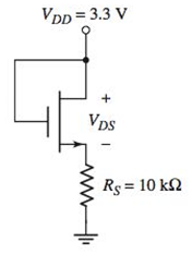
Figure 3.43 Circuit for Exercise TYU 3.8
Expert Solution & Answer
Want to see the full answer?
Check out a sample textbook solution
Students have asked these similar questions
In the voltage divider bias circuit shown, R1 = 8 kΩ R2=2 kΩ, RC=3.5 kΩ, RE=2 kΩ, VCC=13.5 V. Assuming a stiff voltage divider bias, calculate the following (βDC=100):
Base voltage.
Emitter Voltage.
Emitter current.
Collector Voltage.
Collector to emitter voltage.
An npn transistor has the CE input characteristics shown in Figure 3-19 (p. 115) and the CE output characteristics shown in Figure 3-20 (p. 115).
(a) Find IB when VBE = 0.7 V and VCE = 20 V.
(b) Find the beta of the transistor at VCE = 6.0 V and IB = 20uA (neglecting leakage).
(c) Find bac for VCE = 6.0V and IB varying from 20 uA to 40 uA.
(d) What is the approximate value of VCE,sat in Fig. 3-20?
The switches as shown can be implementedusing MOSFETs, as shown. Whatare the W/L ratios of the transistors if the onresistanceof the transistor is to be less than 1 percentof the resistor 2R = 10 kohm ? Assume thatthe voltage applied to the gate of the MOSFET is5 V when b1 = 1 and 0 V when b1 = 0. For theMOSFET, VTN = 1 V, K'n= 50 A/V2, 2φF = 0.6V, and γ = 0.5√V.
Chapter 3 Solutions
Microelectronics: Circuit Analysis and Design
Ch. 3 - An NMOS transistor with VTN=1V has a drain current...Ch. 3 - An PMOS device with VTP=1.2V has a drain current...Ch. 3 - (a) An nchannel enhancementmode MOSFET has a...Ch. 3 - The NMOS devices described in Exercise TYU 3.1...Ch. 3 - (a) A pchannel enhancementmode MOSFET has a...Ch. 3 - The PMOS devices described in Exercise TYU 3.3...Ch. 3 - The parameters of an NMOS enhancementmode device...Ch. 3 - An NMOS transistor has parameters VTNO=0.4V ,...Ch. 3 - Prob. 3.3EPCh. 3 - The transistor in Figure 3.26(a) has parameters...
Ch. 3 - For the transistor in the circuit in Figure 3.28,...Ch. 3 - Consider the circuit shown in Figure 3.30. The...Ch. 3 - Consider the circuit in Figure 3.30. Using the...Ch. 3 - (a) Consider the circuit shown in Figure 3.33. The...Ch. 3 - Consider the NMOS inverter shown in Figure 3.36...Ch. 3 - Consider the circuit shown in Figure 3.39 with...Ch. 3 - Consider the circuit in Figure 3.41. Assume the...Ch. 3 - Prob. 3.7TYUCh. 3 - Consider the circuit in Figure 3.43. The...Ch. 3 - For the circuit shown in Figure 3.36, use the...Ch. 3 - Consider the circuit shown in Figure 3.44. The...Ch. 3 - For the circuit shown in Figure 3.39, use the...Ch. 3 - For the MOS inverter circuit shown in Figure 3.45,...Ch. 3 - For the circuit in Figure 3.46, assume the circuit...Ch. 3 - The circuit shown in Figure 3.45 is biased at...Ch. 3 - The transistor in the circuit shown in Figure 3.48...Ch. 3 - In the circuit in Figure 3.46, let RD=25k and...Ch. 3 - For the circuit shown in Figure 3.49(a), assume...Ch. 3 - Prob. 3.15EPCh. 3 - Consider the constantcurrent source shown in...Ch. 3 - Consider the circuit in Figure 3.49(b). Assume...Ch. 3 - Consider the circuit shown in Figure 3.50. Assume...Ch. 3 - The transistor parameters for the circuit shown in...Ch. 3 - The transistor parameters for the circuit shown in...Ch. 3 - The parameters of an nchannel JFET are IDSS=12mA ,...Ch. 3 - The transistor in the circuit in Figure 3.62 has...Ch. 3 - For the pchannel transistor in the circuit in...Ch. 3 - Consider the circuit shown in Figure 3.66 with...Ch. 3 - The nchannel enhancementmode MESFET in the circuit...Ch. 3 - For the inverter circuit shown in Figure 3.68, the...Ch. 3 - Describe the basic structure and operation of a...Ch. 3 - Sketch the general currentvoltage characteristics...Ch. 3 - Describe what is meant by threshold voltage,...Ch. 3 - Describe the channel length modulation effect and...Ch. 3 - Describe a simple commonsource MOSFET circuit with...Ch. 3 - Prob. 6RQCh. 3 - In the dc analysis of some MOSFET circuits,...Ch. 3 - Prob. 8RQCh. 3 - Describe the currentvoltage relation of an...Ch. 3 - Describe the currentvoltage relation of an...Ch. 3 - Prob. 11RQCh. 3 - Describe how a MOSFET can be used to amplify a...Ch. 3 - Describe the basic operation of a junction FET.Ch. 3 - Prob. 14RQCh. 3 - (a) Calculate the drain current in an NMOS...Ch. 3 - The current in an NMOS transistor is 0.5 mA when...Ch. 3 - The transistor characteristics iD versus VDS for...Ch. 3 - For an nchannel depletionmode MOSFET, the...Ch. 3 - Verify the results of Example 3.4 with a PSpice...Ch. 3 - The threshold voltage of each transistor in Figure...Ch. 3 - The threshold voltage of each transistor in Figure...Ch. 3 - Consider an nchannel depletionmode MOSFET with...Ch. 3 - Determine the value of the process conduction...Ch. 3 - An nchannel enhancementmode MOSFET has parameters...Ch. 3 - Consider the NMOS circuit shown in Figure 3.36....Ch. 3 - An NMOS device has parameters VTN=0.8V , L=0.8m ,...Ch. 3 - Consider the NMOS circuit shown in Figure 3.39....Ch. 3 - A particular NMOS device has parameters VTN=0.6V ,...Ch. 3 - MOS transistors with very short channels do not...Ch. 3 - For a pchannel enhancementmode MOSFET, kp=50A/V2 ....Ch. 3 - For a pchannel enhancementmode MOSFET, the...Ch. 3 - The transistor characteristics iD versus SD for a...Ch. 3 - A pchannel depletionmode MOSFET has parameters...Ch. 3 - Calculate the drain current in a PMOS transistor...Ch. 3 - sDetermine the value of the process conduction...Ch. 3 - Enhancementmode NMOS and PMOS devices both have...Ch. 3 - For an NMOS enhancementmode transistor, the...Ch. 3 - The parameters of an nchannel enhancementmode...Ch. 3 - An enhancementmode NMOS transistor has parameters...Ch. 3 - An NMOS transistor has parameters VTO=0.75V ,...Ch. 3 - (a) A silicon dioxide gate insulator of an MOS...Ch. 3 - In a power MOS transistor, the maximum applied...Ch. 3 - In the circuit in Figure P3.26, the transistor...Ch. 3 - The transistor in the circuit in Figure P3.27 has...Ch. 3 - Prob. D3.28PCh. 3 - The transistor in the circuit in Figure P3.29 has...Ch. 3 - Consider the circuit in Figure P3.30. The...Ch. 3 - For the circuit in Figure P3.31, the transistor...Ch. 3 - Design a MOSFET circuit in the configuration shown...Ch. 3 - Consider the circuit shown in Figure P3.33. The...Ch. 3 - The transistor parameters for the transistor in...Ch. 3 - For the transistor in the circuit in Figure P3.35,...Ch. 3 - Design a MOSFET circuit with the configuration...Ch. 3 - The parameters of the transistors in Figures P3.37...Ch. 3 - For the circuit in Figure P3.38, the transistor...Ch. 3 - Prob. 3.39PCh. 3 - Prob. 3.40PCh. 3 - Design the circuit in Figure P3.41 so that...Ch. 3 - Prob. 3.42PCh. 3 - Prob. 3.43PCh. 3 - Prob. 3.44PCh. 3 - Prob. 3.45PCh. 3 - Prob. 3.46PCh. 3 - Prob. 3.47PCh. 3 - The transistors in the circuit in Figure 3.36 in...Ch. 3 - For the circuit in Figure 3.39 in the text, the...Ch. 3 - Prob. 3.50PCh. 3 - The transistor in the circuit in Figure P3.51 is...Ch. 3 - Prob. 3.52PCh. 3 - For the twoinput NMOS NOR logic gate in Figure...Ch. 3 - All transistors in the currentsource circuit shown...Ch. 3 - All transistors in the currentsource circuit shown...Ch. 3 - Consider the circuit shown in Figure 3.50 in the...Ch. 3 - The gate and source of an nchannel depletionmode...Ch. 3 - For an nchannel JFET, the parameters are IDSS=6mA...Ch. 3 - A pchannel JFET biased in the saturation region...Ch. 3 - Prob. 3.60PCh. 3 - Prob. 3.61PCh. 3 - The threshold voltage of a GaAs MESFET is...Ch. 3 - Prob. 3.63PCh. 3 - Prob. 3.64PCh. 3 - Prob. 3.65PCh. 3 - For the circuit in Figure P3.66, the transistor...Ch. 3 - Prob. 3.67PCh. 3 - Prob. 3.68PCh. 3 - For the circuit in Figure P3.69, the transistor...Ch. 3 - Prob. 3.70PCh. 3 - Prob. 3.71PCh. 3 - Prob. 3.72PCh. 3 - Using a computer simulation, verify the results of...Ch. 3 - Consider the PMOS circuit shown in Figure 3.30....Ch. 3 - Consider the circuit in Figure 3.39 with a...Ch. 3 - Prob. D3.79DPCh. 3 - Consider the multitransistor circuit in Figure...
Knowledge Booster


Learn more about
Need a deep-dive on the concept behind this application? Look no further. Learn more about this topic, electrical-engineering and related others by exploring similar questions and additional content below.Similar questions
- Prepare the comparison table for the Power semiconductor devices 1)Integrated gate-commutated thyristor (IGCT) 2) Static induction thyristor (SITH) 3)Static induction transistor (SIT) .(Symbol, VI characteristics, Application, Voltage & Current rating)arrow_forwardMoore’s Law states that the number of transistors in an integrated circuit doubles every two years. What do you think is the implication of doubling the number of transistors?arrow_forwardFor an NPN Bipolar Junction Transistor base-emitter voltage, VBE is 0.7 V at collector current,Ic of 1mA. Calculate the saturation current, emitter-base voltage, emitter current whencollector current is (X+2) mA. Assume β =100 and T=300 K for your calculation.arrow_forward
- The mode of operation for the D-MOSFET is Select one: a. the ohmic region only b. the enhancement mode only c. both the depletion and enhancement modes d. the depletion mode onlyarrow_forwardShow that the drain current IDQ is approximately equal to 3.65 mA (graphically or otherwise). Then calculate VDSQ.arrow_forwardA bipolar NPN transistor has a DC Beta of 200mA. Calculate the base current IB required to switch a resistive (collector) load of 5000µA Please show solution Choices: 20µA0.25mA0.025mA250µAarrow_forward
- Calculate Ic, Vcc, β, and RB for the circuit shown belowarrow_forwardThe channel resistance of a MOSFET can be computed by getting the reciprocal of the derivative of the drain current with respect to the drain to source voltage. Compute the channel resistance (in Ω) of an NMOS operating in the linear region given the following MOSFET specifications: k = 2.39μA/V2, W/L = 157, VGS = 4V, VTH = 0.90V, and VDS = 0.24V.arrow_forwardQ3) Bring out the advantages and disadvantages of microwave tube devices and semiconductor devices. What are the most common types of microwave diodes and transistors in use give their basic features and applications? What are the most common types of microwave ICs? Give details of the circuit elements and applicationsarrow_forward
- Q3:Choose One of the following: : (A)In common emmiter voltage divider bias of BJT, Vcc = 25V; R1= 10 k ohm; R2, = 2.2 k ohm ;Rc = 3.6 k ohm and RE = 1 k ohm.Determain Vec at ß = 120.using Exact analysis Draw the equvelent circuit inaddition the DC load line curve . (B)For self bais(Emitter resistace bais) of BJT,Vcc= 22 V, lb = 45macroA, a = 0.99, RE = 1 k ohm. Determain VCe Draw the equvelent circuit inaddition to DC load line curve.arrow_forwardFor the NMOSFET, K=2mA/V^2 and V_THN = 1V. Determine the current I_Rarrow_forward( b ) For the Junction Field Effect Transistor ( JFET ) shown in Figure Q1 ( b ) below , given that maximum current Ipss = 10 mA , pinch - off voltage Vp = -5 V , R D= 2 ka , source voltage and resistance are VDD= 12 V and Rs = 5 kn , respectively , solve to determine following (i) The quiescent voltage between the gate and source VGSQ . (ii) The quiescent drain current IDQarrow_forward
arrow_back_ios
SEE MORE QUESTIONS
arrow_forward_ios
Recommended textbooks for you
 Introductory Circuit Analysis (13th Edition)Electrical EngineeringISBN:9780133923605Author:Robert L. BoylestadPublisher:PEARSON
 Delmar's Standard Textbook Of ElectricityElectrical EngineeringISBN:9781337900348Author:Stephen L. HermanPublisher:Cengage Learning
 Programmable Logic ControllersElectrical EngineeringISBN:9780073373843Author:Frank D. PetruzellaPublisher:McGraw-Hill Education
 Fundamentals of Electric CircuitsElectrical EngineeringISBN:9780078028229Author:Charles K Alexander, Matthew SadikuPublisher:McGraw-Hill Education
 Electric Circuits. (11th Edition)Electrical EngineeringISBN:9780134746968Author:James W. Nilsson, Susan RiedelPublisher:PEARSON
 Engineering ElectromagneticsElectrical EngineeringISBN:9780078028151Author:Hayt, William H. (william Hart), Jr, BUCK, John A.Publisher:Mcgraw-hill Education,
Introductory Circuit Analysis (13th Edition)
Electrical Engineering
ISBN:9780133923605
Author:Robert L. Boylestad
Publisher:PEARSON
Delmar's Standard Textbook Of Electricity
Electrical Engineering
ISBN:9781337900348
Author:Stephen L. Herman
Publisher:Cengage Learning
Programmable Logic Controllers
Electrical Engineering
ISBN:9780073373843
Author:Frank D. Petruzella
Publisher:McGraw-Hill Education
Fundamentals of Electric Circuits
Electrical Engineering
ISBN:9780078028229
Author:Charles K Alexander, Matthew Sadiku
Publisher:McGraw-Hill Education
Electric Circuits. (11th Edition)
Electrical Engineering
ISBN:9780134746968
Author:James W. Nilsson, Susan Riedel
Publisher:PEARSON
Engineering Electromagnetics
Electrical Engineering
ISBN:9780078028151
Author:Hayt, William H. (william Hart), Jr, BUCK, John A.
Publisher:Mcgraw-hill Education,
Diode Logic Gates - OR, NOR, AND, & NAND; Author: The Organic Chemistry Tutor;https://www.youtube.com/watch?v=9lqwSaIDm2g;License: Standard Youtube License