
(a)
Interpretation:
From the given pictures, the material that relates to it has to be identified.
Concept introduction:
Semiconductor: A material which can conduct electricity in range between a metal and an insulator is known as semiconductor. Addition of small amount of impurities increases conductivity of semiconductor and the process is known as doping. n-type and p-type are two types of doped semiconductors.
n-type: This is a type of doped semiconductor in which many free electrons are present in conduction band.
p-type: This is a type of doped semiconductor in which holes are present in conduction band.
Insulator: Insulators are one, in which electrons are filled in valence band with a vacant conduction band and they are parted away by band gap.
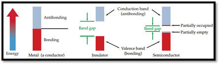
Figure 1
(b)
Interpretation:
The ascending order of electrical conductivity of given materials has to be arranged and explained.
Concept introduction:
Semiconductor: A material which can conduct electricity in range between a metal and an insulator is known as semiconductor. Addition of small amount of impurities increases conductivity of semiconductor and the process is known as doping. n-type and p-type are two types of doped semiconductors.
n-type: This is a type of doped semiconductor in which many free electrons are present in conduction band.
p-type: This is a type of doped semiconductor in which holes are present in conduction band.
Insulator: Insulators in which electrons are filled in valence band with a vacant conduction band and they are parted away by band gap. Insulators does not conduct electricity.
(c)
Interpretation:
The effect of increase in temperature on the conductivity of given material has to be given.
Concept introduction:
Semiconductor: A material which can conducts electricity in range between a metal and an insulator is known as semiconductor. Addition of small amount of impurities increases conductivity of semiconductor and the process is known as doping. n-type and p-type are two types of doped semiconductors.
n-type: This is a type of doped semiconductor in which many free electrons are present in conduction band.
p-type: This is a type of doped semiconductor in which holes are present in conduction band.
Insulator: Insulators in which electrons are filled in valence band with a vacant conduction band and they are parted away by band gap. Insulators does not conduct electricity.
Effect of change in temperature: Increase in temperature increases electrical conductivity of semiconductors because when temperature raises, there will be more electrons in conduction band and hole in valance band. On the other hand, electrical conductivity decreases when temperature increases due to increased vibrational motion of metal cation around lattice leads to disruption of flow of electrons in crystal.
Want to see the full answer?
Check out a sample textbook solution
Chapter 21 Solutions
General Chemistry: Atoms First

- calculate the linear electron density of gallium arsenide in with is 10 nm the sub band values of the GeAr are nx =2,ny =2arrow_forwardWhat is band broadening? Explain the phenomenon of eddy diffusion.arrow_forwardThe first LEDs were made from GaAs, which has a bandgap of 1.43 eV. What wavelength of light would be emittedfrom an LED made from GaAs? What region of theelectromagnetic spectrum does this light correspond to: ultraviolet,visible, or infrared?arrow_forward
- Sketch the band structure of a Li AND a Si crystal. (ii) How would you expect the electrical conductivity in Li AND Si crystals to vary with temperature? (iii) Account for the fact that the conductivity of Si is enhanced by the addition of small amounts of B.arrow_forwardThe maximum wavelength of light that a certain silicon photocell can detect is 1.11 μm. (a) What is the energy gap (in electron volts) between the valence and conduction bands for this photocell? (b) Explain why pure silicon is opaque.arrow_forwardWhat are the main differences between Diamagnetic and Paramagnetic materials?arrow_forward
- Would you expect carborundum(SiC) to adopt a diamond structure or one of higher coordination? Explain why?arrow_forwardThe nitride ceramics AIN, GaN, and InN are all semiconductors used in the microelectronics industry. Their band gaps are 580.6, 322.1, and 192.9 kJ/mol, respectively. Which, if any, energies correspond to radiation in the visible region of the spectrum ?arrow_forwardWhich of these band diagrams is consistent with diamond being an electrical insulator?Ge is a semiconductor. If half of the Ge atoms of a sample of Ge are replaced with Ga atoms, with what elementshould the other half of the Ga atoms be replaced in order for this new compound to be isoelectronic with Ge?arrow_forward
- 2. Compare and contrast band theory associated with metals, insulator and semiconductors with figures. Include in your essay the effects of heating and cooling on the solids.arrow_forwardWhen you shine light of band gap energy or higher on asemiconductor and promote electrons from the valenceband to the conduction band, do you expect the conductivityof the semiconductor to (a) remain unchanged,(b) increase, or (c) decrease?arrow_forwardIs Aluminium is commonly deliberately alloyed with iron? Why ?arrow_forward
 Principles of Modern ChemistryChemistryISBN:9781305079113Author:David W. Oxtoby, H. Pat Gillis, Laurie J. ButlerPublisher:Cengage Learning
 Chemistry for Engineering StudentsChemistryISBN:9781337398909Author:Lawrence S. Brown, Tom HolmePublisher:Cengage Learning
 Organic ChemistryChemistryISBN:9781305580350Author:William H. Brown, Brent L. Iverson, Eric Anslyn, Christopher S. FootePublisher:Cengage Learning