Microelectronics: Circuit Analysis and Design
4th Edition
ISBN: 9780073380643
Author: Donald A. Neamen
Publisher: McGraw-Hill Companies, The
bartleby

Videos

Textbook Question
Book Icon
Chapter 8, Problem 8.22P

Consider an idealized class−B output stage shown in Figure P8.22. (The effective turn−on voltages of devices A and B are zero, and the effective “saturation” voltages of
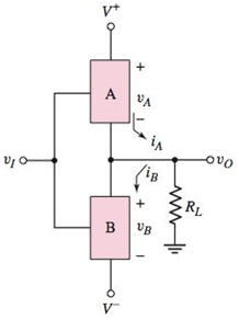
 υ A and υ B are zero.) Assume V + =5V and V =-5V . Assume a symmetrical sine wave is produced at the output. (a) What is the peak output voltage at maximum power conversion efficiency? (b) What is the peak output voltage when each device dissipates the maximum power? (c) If the maximum allowed power dissipation in each device is 2 W and the output voltage is at its maximum value, what is the smaller permitted value of output load resistance?

Chapter 8, Problem 8.22P, Consider an idealized classB output stage shown in Figure P8.22. (The effective turnon voltages of
Figure P8.22

Blurred answer
Students have asked these similar questions
For an electrical engineer point of view, write the following :
Build an AC/DC dual power supply circuit that draws a 60Vp-p sinusoidal voltage, to provide a dc output voltage of +15 V. Full analysis of voltages and currents should be included. What modifications would you recommend to draw more current while maintaining same output voltage?
Draw a three-phase full-wave fully controlled AC / DC converter circuit, describe the operating principle and write the integral correlation that gives the average value of the DC output voltage at any t1 moment

Chapter 8 Solutions

Microelectronics: Circuit Analysis and Design

Ch. 8 - Prob. 8.5TYUCh. 8 - Prob. 8.6TYUCh. 8 - A transformercoupled emitterfollower amplifier is...Ch. 8 - Prob. 8.7TYUCh. 8 - Prob. 8.9EPCh. 8 - Prob. 8.11EPCh. 8 - Consider the classAB output stage shown in Figure...Ch. 8 - From Figure 8.36, show that the overall current...Ch. 8 - Prob. 1RQCh. 8 - Describe the safe operating area for a transistor.Ch. 8 - Why is an interdigitated structure typically used...Ch. 8 - Discuss the role of thermal resistance between...Ch. 8 - Define and describe the power derating curve for a...Ch. 8 - Define power conversion efficiency for an output...Ch. 8 - Prob. 7RQCh. 8 - Describe the operation of an ideal classB output...Ch. 8 - Discuss crossover distortion.Ch. 8 - What is meant by harmonic distortion?Ch. 8 - Describe the operation of a classAB output stage...Ch. 8 - Describe the operation of a transformercoupled...Ch. 8 - Prob. 13RQCh. 8 - Sketch a classAB complementary MOSFET pushpull...Ch. 8 - What are the advantages of a Darlington pair...Ch. 8 - Sketch a twotransistor configuration using npn and...Ch. 8 - Prob. 8.1PCh. 8 - Prob. 8.2PCh. 8 - Prob. 8.3PCh. 8 - Prob. 8.4PCh. 8 - Prob. 8.5PCh. 8 - Prob. D8.6PCh. 8 - A particular transistor is rated for a maximum...Ch. 8 - Prob. 8.8PCh. 8 - For a power MOSFET, devcase=1.5C/W , snkamb=2.8C/W...Ch. 8 - Prob. 8.10PCh. 8 - The quiescent collector current in a BiT is ICQ=3A...Ch. 8 - Prob. 8.12PCh. 8 - Prob. 8.13PCh. 8 - Prob. 8.14PCh. 8 - Prob. 8.15PCh. 8 - Prob. 8.16PCh. 8 - Consider the classA sourcefollower circuit shown...Ch. 8 - Prob. 8.18PCh. 8 - Prob. 8.19PCh. 8 - Prob. 8.20PCh. 8 - Prob. 8.21PCh. 8 - Consider an idealized classB output stage shown in...Ch. 8 - Consider an idealized classB output stage shown in...Ch. 8 - Prob. 8.24PCh. 8 - For the classB output stage shown in Figure P8.24,...Ch. 8 - Prob. 8.26PCh. 8 - Prob. 8.27PCh. 8 - Consider the classAB output stage in Figure P8.28....Ch. 8 - Prob. 8.29PCh. 8 - Prob. D8.30PCh. 8 - Prob. 8.31PCh. 8 - Prob. D8.32PCh. 8 - Consider the transformercoupled commonemitter...Ch. 8 - The parameters for the transformercoupled...Ch. 8 - A BJT emitter follower is coupled to a load with...Ch. 8 - Consider the transformercoupled emitter follower...Ch. 8 - A classA transformer-coupled emitter follower must...Ch. 8 - Repeat Problem 8.36 if the primary side of the...Ch. 8 - Consider the circuit in Figure 8.31. The circuit...Ch. 8 - Prob. D8.40PCh. 8 - The value of IBiass in the circuit shown in Figure...Ch. 8 - The transistors in the output stage in Figure 8.34...Ch. 8 - Consider the circuit in Figure 8.34. The supply...Ch. 8 - Prob. 8.44PCh. 8 - Prob. 8.45PCh. 8 - Consider the classAB MOSFET output stage shown in...Ch. 8 - Prob. 8.47PCh. 8 - Consider the classAB output stage in Figure P8.48....Ch. 8 - For the classAB output stage in Figure 8.36, the...
Knowledge Booster
Background pattern image
Electrical Engineering
Learn more about
Need a deep-dive on the concept behind this application? Look no further. Learn more about this topic, electrical-engineering and related others by exploring similar questions and additional content below.
Recommended textbooks for you
Text book image
Introductory Circuit Analysis (13th Edition)
Electrical Engineering
ISBN:9780133923605
Author:Robert L. Boylestad
Publisher:PEARSON
Text book image
Delmar's Standard Textbook Of Electricity
Electrical Engineering
ISBN:9781337900348
Author:Stephen L. Herman
Publisher:Cengage Learning
Text book image
Programmable Logic Controllers
Electrical Engineering
ISBN:9780073373843
Author:Frank D. Petruzella
Publisher:McGraw-Hill Education
Text book image
Fundamentals of Electric Circuits
Electrical Engineering
ISBN:9780078028229
Author:Charles K Alexander, Matthew Sadiku
Publisher:McGraw-Hill Education
Text book image
Electric Circuits. (11th Edition)
Electrical Engineering
ISBN:9780134746968
Author:James W. Nilsson, Susan Riedel
Publisher:PEARSON
Text book image
Engineering Electromagnetics
Electrical Engineering
ISBN:9780078028151
Author:Hayt, William H. (william Hart), Jr, BUCK, John A.
Publisher:Mcgraw-hill Education,
Diode Logic Gates - OR, NOR, AND, & NAND; Author: The Organic Chemistry Tutor;https://www.youtube.com/watch?v=9lqwSaIDm2g;License: Standard Youtube License