
Videos
Consider the class−AB output stage shown in Figure 8.37. The transistor parameters are
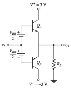
Figure 8.37 Figure for Exercise TYU 8.8
Want to see the full answer?
Check out a sample textbook solution
Chapter 8 Solutions
Microelectronics: Circuit Analysis and Design


- In the context of MOS devices, state briefly the advantages of:(a) constant field scaling(b) high-κ dielectrics(c) mid-gap metalsarrow_forwardIn the circuit in the figure, VGSQ = 6.8 V, IDQ = 2.4 mA, VGS(Th) = 3.3 V, k = 0.4x10⁻³ A/V2, RD = 5.6 kΩ, RF = 2.2 MΩ and rd = 25 kΩ. Accordingly, when a RL = 0.1 kΩ load is connected to the output of the circuit, what will be the voltage gain of the circuit? NOTE: MOSFET output resistance must be taken into account in rd calculationsarrow_forwardConsider a CE circuit, where trans-conductance is 50mΩ-1, diffusion capacitance is 100 pF, transition capacitance is 3 pF. IB = 20μA. Given base emitter dynamic resistance, rbe = 1000 Ω, input VI is 20*sin(107t). What is the short circuit current gain?arrow_forward
- The LED in Figure below requires 30 mA to emit a sufficient level of light. Therefore, the collector current should be approximately 30 mA. For the following circuit values, determine the amplitude of the square wave input voltage necessary to make sure that the transistor saturates. Use double the minimum value of base current as a safety margin to ensure saturation. VCC = 8 V, VCE(sat) = 0.3 V, RC = 200 Ω , RB = 3.3 kΩ , b (beta) = 45, and VLED = 1.6 V.arrow_forwardAn equivalent circuit for a piezoelectric accelerometer, which uses a quartz crystal as the sensing element, is shown in the following figure. The generated charge is denoted by q and the output voltage at the end of the accelerometer cable is vo. The piezoelectric sensor capacitance is modeled by Cp and the overall capacitance experienced at the sensor output, whose primary contribution is due to cable capacitance, is denoted by Cc. The resistance of the electric insulation in the accelerometer is denoted by R. Write a differential equation relating vo to q. What is the corresponding transfer function? Using this result, show that the accuracy of the accelerometer improves when the sensor time constant is large and when the frequency of the measured acceleration is high. For a quartz crystal sensor with R = 1 × 10¹¹ Ω and Cp = 300 pF, and a circuit with Cc = 700 pF, compute the time constant.arrow_forwardFor the transistor , IS = 4 × 10⁻¹⁶ μA,βF = 75, and βR = 4. (a) Label the collector, base,and emitter terminals of the transistor. (b) What isthe transistor type? (c) Label the emitter-base andcollector-base voltages, and label the normal direction for IE , IC, and IB. (d) Write the simplified formof the transport model equations that apply to thisparticular circuit configuration. Write an expressionfor IE /IB. Write an expression for IE /IC. (e) Findthe values of IE , IC, IB, VC B, and VE B.arrow_forward
- Answer as quickly as possible. I'll give upvote. Thank you. The circuit shown is a common source amplifier with a current mirror bias. It is given that the NMOS (M1) parameters are μoCox = 3mA/V2, VTH,n = 0.5V and λ = 0.02 and the PMOS (M2 and M3) parameters are μoCox = 1mA/V2 and VTH,p = −0.6V . The PMOS transistor M3 does not have channel length modulation while PMOS transistor M2 has λ = 0.02. It is also given that the dimensions of M2 and M3 have equal widths of 5µm and lengths of L2 = 3µm and L3 = 1.5µm, respectively. M1 has length of L1 = 1µm and width of W1 = 2µm. Find the gm and ro of transistor M1.arrow_forwardA GaAlAs LED with an active region width of 1.5 μm operates at 300K at a current density of 120A/cm2. Assuming that the steady state electron density is n=1017 cm-3calculate the carrier lifetime. Also calculate the optical 3-dB cut-off frequencyarrow_forwardSince IDSS=8 mA, VGS(off) = -10V according to the circuit on the side, if the capacitor C2 is removed, what will be the Av gain value?arrow_forward
- Design a Single-Stage Common Emitter Class A Amplifier Specifications:Voltage Divider Bias Circuit Supply: Any value from 10Vdc to 24VdcLoad: 1kΩVoltage Gain: Any value from 80 to 400Lower Cutoff Frequency: 100 HzSinusoidal source (zero internal resistance): 50mVp-pTransistor: Si, β = 75 • Base-Collector capacitance = 8pF • Base-Emitter Capacitance = 25pF a) compute for the biasing resistances.b) determine the dc transistor terminal voltages and transistor currents.arrow_forwardFind 1) If a capacitor Cs is connected across Rs then Av= 2) The value of RD required to set Q-pt at center of saturation Regn. RD= 3) The max. undistorted peak value for vds = Electronics 2arrow_forwardDesign for an efficient 8x1 multiplexer (MUX) using CMOS technology. The primary goal is to optimize the area and power consumption while ensuring the proper functionality of the multiplexer. Utilize transmission gate technology as a part of the design process. Balance between transistor count, power efficiency, and space utilization. Note: The design should not only be functional but also efficient in terms of power and space usage, demonstrating a deep understanding of CMOS technology and multiplexer design principles.arrow_forward
 Introductory Circuit Analysis (13th Edition)Electrical EngineeringISBN:9780133923605Author:Robert L. BoylestadPublisher:PEARSON
 Delmar's Standard Textbook Of ElectricityElectrical EngineeringISBN:9781337900348Author:Stephen L. HermanPublisher:Cengage Learning
 Programmable Logic ControllersElectrical EngineeringISBN:9780073373843Author:Frank D. PetruzellaPublisher:McGraw-Hill Education
 Fundamentals of Electric CircuitsElectrical EngineeringISBN:9780078028229Author:Charles K Alexander, Matthew SadikuPublisher:McGraw-Hill Education
 Electric Circuits. (11th Edition)Electrical EngineeringISBN:9780134746968Author:James W. Nilsson, Susan RiedelPublisher:PEARSON
 Engineering ElectromagneticsElectrical EngineeringISBN:9780078028151Author:Hayt, William H. (william Hart), Jr, BUCK, John A.Publisher:Mcgraw-hill Education,