
Concept explainers
Videos
(a)
The transition points for the p-channel and the n-channel MOSFET.
To sketch: The voltage transfer characteristics.
To find: The value of the input voltage for the different values of the input output voltages.
(a)
Answer to Problem 16.32P
The value of the transition voltages are
Explanation of Solution
Calculation:
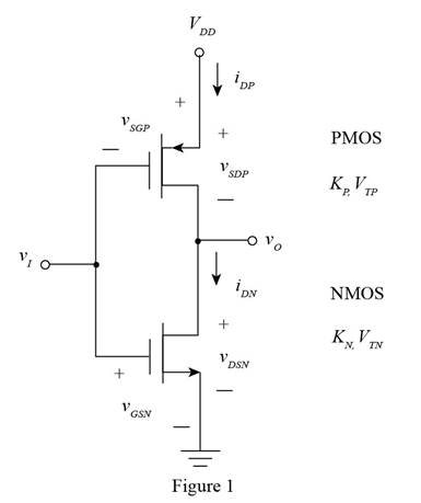
The given diagram is shown in Figure 1
The expression to determine the trans-conductance parameter for NMOS is given by,
Substitute
The expression to determine the trans-conductance parameter for PMOS is given by,
Substitute
The expression to determine the transition points
Substitute
The expression to determine the value of the voltage
Substitute
The expression to determine the value of the voltage
Substitute
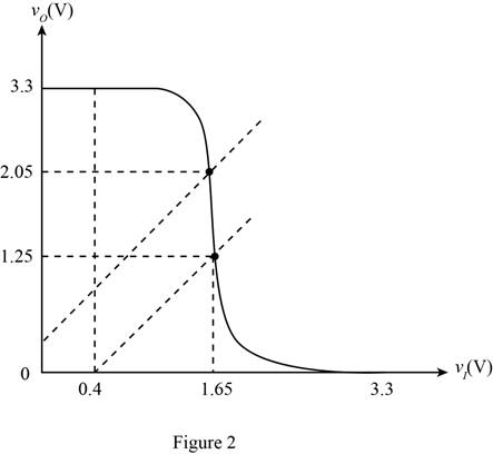
The voltage transfer characteristics is shown below.
The required diagram is shown in Figure 2
The expression to determine the value of the input voltage is given by,
Substitute
The value of the voltage must be less than the supply voltage, thus the input voltage is
The expression to determine the value of the input voltage when the output voltage is more than
Substitute
Conclusion:
Therefore, the value of the transition voltages are
(b)
The transition points for the p-channel and the n-channel MOSFET.
To sketch: The voltage transfer characteristics.
To find: The value of the input voltage for the different values of the input output voltages.
(b)
Answer to Problem 16.32P
The value of the transition voltages are
Explanation of Solution
Calculation:
The expression to determine the trans-conductance parameter for NMOS is given by,
Substitute
The expression to determine the trans-conductance parameter for PMOS is given by,
Substitute
The expression to determine the transition points
Substitute
The expression to determine the value of the voltage
Substitute
The expression to determine the value of the voltage
Substitute
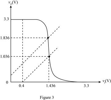
The voltage transfer characteristics is shown below.
The required diagram is shown in Figure 3
The expression to determine the value of the input voltage is given by,
Substitute
The value of the voltage must be less than the supply voltage, thus the input voltage is
The expression to determine the value of the input voltage when the output voltage is more than
Substitute
Conclusion:
Therefore, the value of the transition voltages are
Want to see more full solutions like this?
Chapter 16 Solutions
Microelectronics: Circuit Analysis and Design


- Wire delay I. Calculate the delay of a 10 mm wire in 28 nm technology that is divided into 20 0.5 mm segments with a 20× minimum-size inverter driving each segment.arrow_forwardDescribe the C-V characteristics of a MOS capacitor and explain the physics behind them. 2. Draw the IV curve of a MOSFET for different gate voltages. Explain the characteristics of the curve and dependence on the gate voltage. 3. Explain the structure and operation principle of a CMOS inverter. What are its benefits? 4. Compare SRAM, DRAM and Flash memoriesarrow_forwardDesign an asymmetrical inverter to meet the delay specification a symmetrical CMOS reference inverter to provide a propagation delay of 400 ps fora load capacitance of 200 fF. Use VDD =2.5 V, VTN =0.60 V, and VTP =−0.60 V.with (W/L)P = (W/L)N .arrow_forward
- Five identical inverters are connected in a chain. The low-to-high propagation delay of the inverter is 12ns while the high-to-low propagation delay is 10ns. The input at the first inverter is changed from 1 to 0 at time t=0ns. How long will it take before the output of the 5th inverter change from 0 to 1?arrow_forward(a) A CMOS inverter has (W/L)N =2/1,(W/L)P =5/1, and VDD =3.3 V. Assume VTN =−VTP =0.8 V. What is the peak current in the logicgate and at what input voltage does it occur? (b) Repeatfor VDD =2.0 V with VTN = −VTP = 0.5 V.arrow_forwardWhat are the noise margins of a minimum size CMOS inverter in which both W/L ratios are 2/1 and VDD = 2.5 V and VTN = −VTP = 0.6 V?arrow_forward
- Implement the following functions with two 4-to-1-line multiplexers and a single inverter. F(X, Y, Z) = Σm(1, 2, 3, 6) G(X, Y, Z) = Σm(5, 7) Create the truth table for the two functions. Implement the two functions with two 4-to-1-line multiplexers and a single inverterarrow_forwardIf,for a single phase half bridge inverter the amplitude of output voltage is Vs and the output power is P then their corresponding values for a single phase full-bridge inverter are a. 2Vs,2P b. 2Vs,4P c. 2Vs,P d. Vs,Parrow_forwardGiven Vdd=3.3V, Kn=100uA/V2 , Kp=20uA/V2,Vtn = 0.6V, and Vtp = -0.6V. Determine the Voltage Transfer Characteristics points indicated by the pseudo-NMOS inverter circuit.arrow_forward
- Suppose a ring oscillator is built from N inverters connected in a loop. Each inverter has a minimum delay of tcd and a maximum delay of tpd. If N is odd, determine the range of frequencies at which the oscillator might operate.arrow_forwardPlease can you explain why a 13-bit analogue-to digital-convertor (ADC) is often used in pulse code modulation (PCM) when only 8-bits are transmitted. Then, why following compression in PCM, how and why is an inverter used?arrow_forwardA CMOS inverter is to be designed to drive a single TTL inverter . When vO = VL , the CMOS inverter must sink a current of 1.5 mA and maintain VL ≤0.6 V.When vO ≥ VH , the CMOS inverter must source a current of 60 A and maintain VH ≥2.4 V. What are the minimum W/L ratios of the NMOS and PMOS transistors required to meet these specifications?Assume VDD = 5 V.arrow_forward
 Introductory Circuit Analysis (13th Edition)Electrical EngineeringISBN:9780133923605Author:Robert L. BoylestadPublisher:PEARSON
 Delmar's Standard Textbook Of ElectricityElectrical EngineeringISBN:9781337900348Author:Stephen L. HermanPublisher:Cengage Learning
 Programmable Logic ControllersElectrical EngineeringISBN:9780073373843Author:Frank D. PetruzellaPublisher:McGraw-Hill Education
 Fundamentals of Electric CircuitsElectrical EngineeringISBN:9780078028229Author:Charles K Alexander, Matthew SadikuPublisher:McGraw-Hill Education
 Electric Circuits. (11th Edition)Electrical EngineeringISBN:9780134746968Author:James W. Nilsson, Susan RiedelPublisher:PEARSON
 Engineering ElectromagneticsElectrical EngineeringISBN:9780078028151Author:Hayt, William H. (william Hart), Jr, BUCK, John A.Publisher:Mcgraw-hill Education,