
Concept explainers
Videos
(a)
The maximum allowed tolerance in the
(a)
Answer to Problem 16.99P
The maximum allowed value of the tolerance is
Explanation of Solution
Calculation:
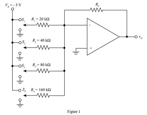
The given diagram is shown in Figure 1
The expression to determine the analog output voltage
Substitute
The expression to determine the value of the least significant digit is given by,
Substitute
The expression to determine the value of the output analog voltage with maximum error is given by,
Substitute
The expression to determine the value of the output analog voltage with maximum error
Substitute
Substitute
The expression to determine the percentage allowed tolerance in the value of resistance
Substitute
Substitute
Substitute
Conclusion:
Therefore, the maximum allowed value of the tolerance is
(b)
The maximum allowed tolerance in the value of
(b)
Answer to Problem 16.99P
The maximum allowed value of the tolerance is
Explanation of Solution
Calculation:
The expression to determine the analog output voltage
Substitute
The expression to determine the value of the output analog voltage with maximum error is given by,
Substitute
The expression to determine the value of the output analog voltage with maximum error
Substitute
Substitute
The expression to determine the percentage allowed tolerance in the value of resistance
Substitute
Substitute
Substitute
Conclusion:
Therefore, the maximum allowed value of the tolerance is
Want to see more full solutions like this?
Chapter 16 Solutions
Microelectronics: Circuit Analysis and Design


- A series resonant inverter with series loaded delivers a load power of P=4000W at resonance. The load resistance is R=10 ohms. The resonant frequency is fo =20 kHz. The input voltage Vs is equal to: Select one: a. None of these b. 160.7V c. 110.1V d. 222.14Varrow_forward1-v(t) = 8cos(2π x160t)+ 4cos(2π x640t) A- Calculate the Nyquist rate for this signal? B- If v(t) is sampled at a rate Ts = 0.001 s what is the resulting discrete time signal v(n)? 2- repeat the Q2 for above v(t) 3- assuming that a3 bit ADC channel accepts analog input 0 to 5 volts, determine A- the no. of quantization levels B- the step size of the quantize C- the quantize level when the analog voltage is 3.2 v D- the binary code produced by the ADCarrow_forwardThe PIC 16F84A microcontroller has a built-in ADC. a. True. b. False.arrow_forward
- 6) Use Mason’s rule to figure out the equivalent input/output transfer functionsarrow_forwardWe are to design a TDM (PCM) link to facilitate the simultaneous transmission of 10 signals. Each signal has a maximum bandwidth of 4 Khz. The PCM encoding system is designed to maintain a signal-to noise (S.N.R) ratio of no worse than 96 dB. What would be the TDM's (1) overall bit rate and (2) bandwidth (assuming the Nyquist bandwith criteria / 2 times bit rate criteria)?. Single choice.arrow_forwardThe output signal to noise ratio for a PCM system is minimum 40 dB. For sinusoidal full scale modulation, estimate the length of the codeword.arrow_forward
- Predict output of a microcontroller with its port P0 connected to LEDs based on the following program. Give your own analysis for each line of the program. BACK: MOV A, #55H MOV P0, A ACALL DELAY MOV A, #0AAH MOV P0, A ACALL DELAY SJMP BACK DELAY: MOV R3, #200 HERE: DJNZ R3, HERE RETarrow_forward1) What is the bit rate that is transmitted by this coder in bits/second? A PCM coder performs an analog‐to‐digital conversion, then transmits the encoded signal over a digital network to a receiver running an equivalent PCM decoder. The PCM encoder runs under the following specifications:- It samples incoming analog signals at 200,000 samples/sec.- It performs uniform quantization on the PAM samples using a –3.2 volt to +3.2 volt scale and 5‐bit quantizationarrow_forwardf(A,B,C,D) = A’B’C + AB’C + ACD + A’B’CD’ +AB’CD’ 1. Optimize the expression above in sum-of-product form using K-Map.2. Write the Shorthand Minterm List.3. From the simplified SOP expression, convert the expression to All-NAND form.arrow_forward
- 1. State the advantages and disadvantages of the DSB-SC modulation.arrow_forwardConsider a digital radio that uses a digital modulation scheme of the 128 QAM type, the width of the allowed radio channel is 40Mhz, determine the maximum speed that could be used in this modulator to meet the bandwidth requirement of the radio channel. RFarrow_forwardQ32) The process of code conversion of the output Of PCM encoder into codes that are suitable for the transmission lines is called a. Line coding b. Mixing c. source coding d. Filtering This multiple choice question from DIGITAL COMMUNICATIONS course.just write for me the final answer.arrow_forward
 Introductory Circuit Analysis (13th Edition)Electrical EngineeringISBN:9780133923605Author:Robert L. BoylestadPublisher:PEARSON
 Delmar's Standard Textbook Of ElectricityElectrical EngineeringISBN:9781337900348Author:Stephen L. HermanPublisher:Cengage Learning
 Programmable Logic ControllersElectrical EngineeringISBN:9780073373843Author:Frank D. PetruzellaPublisher:McGraw-Hill Education
 Fundamentals of Electric CircuitsElectrical EngineeringISBN:9780078028229Author:Charles K Alexander, Matthew SadikuPublisher:McGraw-Hill Education
 Electric Circuits. (11th Edition)Electrical EngineeringISBN:9780134746968Author:James W. Nilsson, Susan RiedelPublisher:PEARSON
 Engineering ElectromagneticsElectrical EngineeringISBN:9780078028151Author:Hayt, William H. (william Hart), Jr, BUCK, John A.Publisher:Mcgraw-hill Education,