
Concept explainers
Videos
To plot: The graphof
To find: The value of
Answer to Problem 16.79P
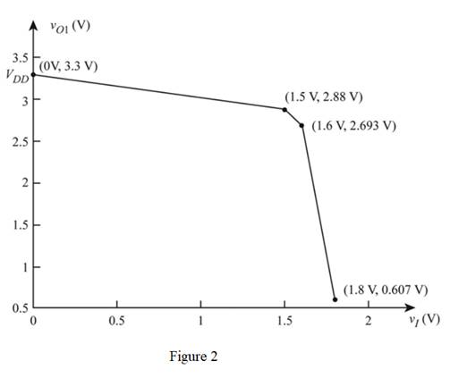
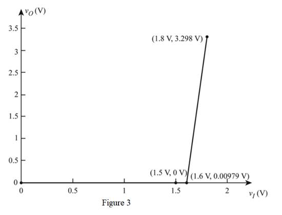
The required plots are shown in Figure 2 and Figure 3. The value of the voltage
Explanation of Solution
Given:
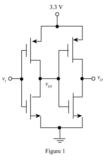
The given diagram is shown in Figure 1.
Calculation:
The expression to determine the transition points
Substitute
Case(i)
The expression to determine the output voltage of the first CMOS inverter is given by,
Substitute
The expression to determine the output voltage of the second CMOS inverter is given by,
Substitute
Thus the value of the of appropriate voltage is
Case (ii)
The expression to determine the output voltage of the first CMOS inverter is given by,
Substitute
The bias voltage is
The expression to determine the output voltage of the second CMOS inverter is given by,
Substitute
Thus the value of the of appropriate voltage is
Case (iii)
The expression to determine the output voltage of the first CMOS inverter is given by,
Substitute
The bias voltage is
The expression to determine the output voltage of the second CMOS inverter is given by,
Substitute
Thus the value of the of appropriate voltage is
Case (iv)
The output voltage of the first and the second CMOS inverter is switching point when the input voltage is the
The plot for the voltage between
The plot between the second CMOS inviter output
The required plot is shown in Figure 3
Conclusion:
Therefore, the required plots are shown in Figure 2 and Figure 3. The value of the voltage
Want to see more full solutions like this?
Chapter 16 Solutions
Microelectronics: Circuit Analysis and Design


- Q/ for Phase shift (Quasi-Square Wave ) PWM inverter, Vdc=100V, L=25mH, R=10ohm, f=60Hz.draw the spectrum of the output voltage and current and then find the output power, rms current value, and the THD . Take n =1-20. What is the effect of increasing and decreasing L on the output current waveform.arrow_forwardDesign an asymmetrical inverter to meet the delay specification a symmetrical CMOS reference inverter to provide a propagation delay of 400 ps fora load capacitance of 200 fF. Use VDD =2.5 V, VTN =0.60 V, and VTP =−0.60 V.with (W/L)P = (W/L)N .arrow_forwardDesign a reference inverter to achieve a delay of 250 ps when driving a 0.2-pF load using a 3.3-V power supply. Assume that the threshold voltages of the CMOS technology are VTN = −VTP = 0.75 V.what W/L ratios are required to actually achieve an average propagation delay of 250 ps?arrow_forward
- Describe the C-V characteristics of a MOS capacitor and explain the physics behind them. 2. Draw the IV curve of a MOSFET for different gate voltages. Explain the characteristics of the curve and dependence on the gate voltage. 3. Explain the structure and operation principle of a CMOS inverter. What are its benefits? 4. Compare SRAM, DRAM and Flash memoriesarrow_forwardSuppose the ECL inverter as shownmust operate at a power of 20 W. If the currentsources are scaled by the same factor, and the capacitancesand voltage levels remain the same, whatis the new propagation delay of the inverter?arrow_forwardCalculate the average propagation delay of the reference inverter in Fig. forC = 1 pF. Repeat for C = 0.2 pF.arrow_forward
- Suppose a ring oscillator is built from N inverters connected in a loop. Each inverter has a minimum delay of tcd and a maximum delay of tpd. If N is odd, determine the range of frequencies at which the oscillator might operate.arrow_forwardHello, I don't konw how to implement expression for part(b) with NAND and NOR gate. My method is : (1) Implement these expression with AND and OR gate. (2) Add bubble in front of the AND gate and add bubble behind the OR gate.Is there anything wrong with my method? Besides, I am wondering why there is a inverter behind the NAND gate (shown in answer1.PNG)Thanks.arrow_forwardFind the ratio of hole mobility to electron mobility of a CMOS inverter given that the beta ratio of pull-up network to pulldown network is 1.5 (Assume that W/L ratio of pMOS is 3 times greater than that of nMOS and all other parameters are same for both) Assuming the supply voltage to be 3V draw a suitable DC transfer characteristic curve of the CMOS inverter.arrow_forward
- (a) What is the power-delay product for a symmetrical CMOS inverterwith (W/L)N =2/1, (W/L)P =5/1, C =0.25 pF,VDD =3.3 V, VTN =0.75 V, and VTP =−0.75 V? (b) Estimate the maximum switchingfrequency for this inverter. (c) Howmuch powerdoes the inverter dissipate if it is switching at thefrequency found in (b)?arrow_forwardA pulse in the positive direction is applied to an inverter. 7 nanoseconds elapse between the leading edge of the input and the leading edge of the output. This parameter is (a) the speed-power product (b) the tPHL propagation delay (c) the tPLH propagation delay (d) the pulse width.arrow_forwardPlot a graph of the voltage transfer characteristicfor an ideal inverter with V+ = 2.5 V, V− = 0 V, andVREF = 0.8 V. Assume VH = V+ and VL = V−.arrow_forward
 Introductory Circuit Analysis (13th Edition)Electrical EngineeringISBN:9780133923605Author:Robert L. BoylestadPublisher:PEARSON
 Delmar's Standard Textbook Of ElectricityElectrical EngineeringISBN:9781337900348Author:Stephen L. HermanPublisher:Cengage Learning
 Programmable Logic ControllersElectrical EngineeringISBN:9780073373843Author:Frank D. PetruzellaPublisher:McGraw-Hill Education
 Fundamentals of Electric CircuitsElectrical EngineeringISBN:9780078028229Author:Charles K Alexander, Matthew SadikuPublisher:McGraw-Hill Education
 Electric Circuits. (11th Edition)Electrical EngineeringISBN:9780134746968Author:James W. Nilsson, Susan RiedelPublisher:PEARSON
 Engineering ElectromagneticsElectrical EngineeringISBN:9780078028151Author:Hayt, William H. (william Hart), Jr, BUCK, John A.Publisher:Mcgraw-hill Education,