
Microelectronics: Circuit Analysis and Design
4th Edition
ISBN: 9780073380643
Author: Donald A. Neamen
Publisher: McGraw-Hill Companies, The
expand_more
expand_more
format_list_bulleted
Videos
Textbook Question
Chapter 16, Problem 16.27P
What is the logic function implemented by the circuit in Figure P16.27.
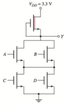
Figure P16.27
Expert Solution & Answer
Want to see the full answer?
Check out a sample textbook solution
Students have asked these similar questions
Perform the functions given below with the decoder given below and a suitable logic gate.
?1(?,?, ?) = ∑m( 3, 5, 6)
?2(?,?, ?) =∑m ( 1, 4)
Sketch the VTC for a logic inverter with VoH = 5 V, Vol = 0.2 V, V.IL= 1.4 V, and VIH= 1.6 V. Also, determine the logic swing , transition width, and the noise margins.
Draw the schematic for a four-input NOR gate witha saturated load device. What are the W/L ratios ofall the transistors, based on the reference inverter ? (b) What is VL if all the logic inputs are equal to 1?
Chapter 16 Solutions
Microelectronics: Circuit Analysis and Design
Ch. 16 - Consider the NMOS inverter with resistor load in...Ch. 16 - The enhancementload NMOS inverter in Figure...Ch. 16 - Prob. 16.3EPCh. 16 - Prob. 16.4EPCh. 16 - Consider the NMOS inverter with enhancement load,...Ch. 16 - Prob. 16.2TYUCh. 16 - (a) Consider the results of Exercise Ex 16.1....Ch. 16 - Prob. 16.5EPCh. 16 - Prob. 16.6EPCh. 16 - (a) Design a threeinput NMOS NOR Logic gate with...
Ch. 16 - Consider the NMOS logic circuit in Figure 16.18....Ch. 16 - Repeat Exercise TYU 16.5 for the NMOS logic...Ch. 16 - The CMOS inverter in Figure 16.21 is biased at...Ch. 16 - swA CMOS inverter is biased at VDD=3V . The...Ch. 16 - A CMOS inverter is biased at VDD=1.8V . The...Ch. 16 - Prob. 16.7TYUCh. 16 - Repeat Exercise Ex 16.9 for a CMOS inverter biased...Ch. 16 - Determine the transistor sizes of a 3input CMOS...Ch. 16 - Design the widthtolength ratios of the transistors...Ch. 16 - Design a static CMOS logic circuit that implements...Ch. 16 - Prob. 16.10TYUCh. 16 - Prob. 16.11TYUCh. 16 - Sketch a clocked CMOS logic circuit that realizes...Ch. 16 - Prob. 16.12EPCh. 16 - Prob. 16.13TYUCh. 16 - Consider the CMOS transmission gate in Figure...Ch. 16 - Prob. 16.15TYUCh. 16 - Prob. 16.14EPCh. 16 - Prob. 16.16TYUCh. 16 - Prob. 16.17TYUCh. 16 - Sketch the quasistatic voltage transfer...Ch. 16 - Sketch an NMOS threeinput NOR logic gate. Describe...Ch. 16 - Discuss how more sophisticated (compared to the...Ch. 16 - Sketch the quasistatic voltage transfer...Ch. 16 - Discuss the parameters that affect the switching...Ch. 16 - Prob. 6RQCh. 16 - Sketch a CMOS threeinput NAND logic gate. Describe...Ch. 16 - sDiscuss how more sophisticated (compared to the...Ch. 16 - Prob. 9RQCh. 16 - Sketch an NMOS transmission gate and describe its...Ch. 16 - Sketch a CMOS transmission gate and describe its...Ch. 16 - Discuss what is meant by pass transistor logic.Ch. 16 - Prob. 13RQCh. 16 - Prob. 14RQCh. 16 - Prob. 15RQCh. 16 - Describe the basic architecture of a semiconductor...Ch. 16 - ‘Sketch a CMOS SRAM cell and describe its...Ch. 16 - Prob. 18RQCh. 16 - Describe a maskprogrammed MOSFET ROM memory.Ch. 16 - Describe the basic operation of a floating gate...Ch. 16 - Prob. 16.1PCh. 16 - Prob. 16.2PCh. 16 - (a) Redesign the resistive load inverter in Figure...Ch. 16 - Prob. D16.4PCh. 16 - Prob. 16.5PCh. 16 - Prob. D16.6PCh. 16 - Prob. 16.7PCh. 16 - Prob. 16.8PCh. 16 - For the depletion load inverter shown in Figure...Ch. 16 - Prob. 16.10PCh. 16 - Prob. D16.11PCh. 16 - Prob. D16.12PCh. 16 - Prob. 16.13PCh. 16 - For the two inverters in Figure P16.14, assume...Ch. 16 - Prob. 16.15PCh. 16 - Prob. 16.16PCh. 16 - Prob. 16.17PCh. 16 - Prob. 16.18PCh. 16 - Prob. D16.19PCh. 16 - Prob. 16.20PCh. 16 - Prob. 16.21PCh. 16 - Prob. 16.22PCh. 16 - In the NMOS circuit in Figure P16.23, the...Ch. 16 - Prob. 16.24PCh. 16 - Prob. 16.25PCh. 16 - Prob. 16.26PCh. 16 - What is the logic function implemented by the...Ch. 16 - Prob. D16.28PCh. 16 - Prob. D16.29PCh. 16 - Prob. 16.31PCh. 16 - Prob. 16.32PCh. 16 - Prob. 16.33PCh. 16 - Consider the CMOS inverter pair in Figure P16.34....Ch. 16 - Prob. 16.35PCh. 16 - Prob. 16.36PCh. 16 - Prob. 16.37PCh. 16 - Prob. 16.38PCh. 16 - Prob. 16.39PCh. 16 - (a) A CMOS digital logic circuit contains the...Ch. 16 - Prob. 16.41PCh. 16 - Prob. 16.42PCh. 16 - Prob. 16.43PCh. 16 - Prob. 16.44PCh. 16 - Prob. 16.45PCh. 16 - Prob. 16.46PCh. 16 - Prob. 16.47PCh. 16 - Prob. 16.48PCh. 16 - Prob. 16.49PCh. 16 - Prob. 16.50PCh. 16 - Prob. 16.51PCh. 16 - Prob. 16.52PCh. 16 - Prob. D16.53PCh. 16 - Figure P16.54 is a classic CMOS logic gate. (a)...Ch. 16 - Figure P16.55 is a classic CMOS logic gate. (a)...Ch. 16 - Consider the classic CMOS logic circuit in Figure...Ch. 16 - (a) Given inputs A,B,C,A,B and C , design a CMOS...Ch. 16 - (a) Given inputs A, B, C, D, and E, design a CMOS...Ch. 16 - (a) Determine the logic function performed by the...Ch. 16 - Prob. D16.60PCh. 16 - Prob. 16.61PCh. 16 - Prob. 16.62PCh. 16 - Sketch a clocked CMOS domino logic circuit that...Ch. 16 - Sketch a clocked CMOS domino logic circuit that...Ch. 16 - Prob. D16.65PCh. 16 - Prob. 16.66PCh. 16 - Prob. 16.67PCh. 16 - The NMOS transistors in the circuit shown in...Ch. 16 - Prob. 16.69PCh. 16 - Prob. 16.70PCh. 16 - Prob. 16.71PCh. 16 - (a) Design an NMOS pass transistor logic circuit...Ch. 16 - Prob. 16.73PCh. 16 - What is the logic function implemented by the...Ch. 16 - Prob. 16.75PCh. 16 - Prob. 16.76PCh. 16 - Prob. 16.77PCh. 16 - Consider the NMOS RS flipflop in Figure 16.63...Ch. 16 - Prob. 16.79PCh. 16 - Consider the circuit in Figure P16.80. Determine...Ch. 16 - Prob. D16.81PCh. 16 - Prob. 16.82PCh. 16 - Prob. 16.83PCh. 16 - Prob. 16.84PCh. 16 - (a) A 1 megabit memory is organized in a square...Ch. 16 - Prob. 16.86PCh. 16 - Prob. 16.87PCh. 16 - Prob. 16.88PCh. 16 - Prob. D16.89PCh. 16 - Prob. 16.90PCh. 16 - Prob. 16.91PCh. 16 - Prob. 16.92PCh. 16 - Prob. D16.93PCh. 16 - Prob. D16.94PCh. 16 - Prob. D16.95PCh. 16 - An analog signal in the range 0 to 5 V is to be...Ch. 16 - Prob. 16.97PCh. 16 - Prob. 16.98PCh. 16 - Prob. 16.99PCh. 16 - The weightedresistor D/A converter in Figure 16.90...Ch. 16 - The Nbit D/A converter with an R2R ladder network...Ch. 16 - Prob. 16.102PCh. 16 - Prob. 16.103PCh. 16 - Prob. 16.104PCh. 16 - Prob. 16.105PCh. 16 - Design a classic CMOS logic circuit that will...Ch. 16 - Prob. D16.111DPCh. 16 - Prob. D16.112DPCh. 16 - Prob. D16.113DP
Knowledge Booster


Learn more about
Need a deep-dive on the concept behind this application? Look no further. Learn more about this topic, electrical-engineering and related others by exploring similar questions and additional content below.Similar questions
- Analyst COMBINATION . Fine Output logic and Equation ?arrow_forwardHow would you manipulate this equation to get it into a format where you can draw it as a NAND and inverter gates logic diagram and a NOR and inverter gates logic diagram?arrow_forwardIntroduce the concept of dynamic logic and domino CMOS logic techniques.arrow_forward
- please explain step by step how to calculate the number of transistors given the logic gates AND, OR, NOT.arrow_forwardDiscuss the pin diagram of any logic gate? Explain how the NAND gate can be used to derive the other logic gates.arrow_forwardSketch the schematic of z in pseudo nmos logicarrow_forward
- (a) A CMOS inverter has (W/L)N =15/1,(W/L)P =15/1, and VDD =3.3V. What is the peakcurrent in the logic gate and at what input voltagedoes it occur? (b) Repeat for VDD =2.5 V.arrow_forwardWhat is the minimum logic swing V required foran ECL gate to have a noise margin of 0.1V at roomtemperature?arrow_forwardHow to do ? Need *State diagram *State/output table *Transition table *Transition equation *Excitation equation and output equation *Logic circuit diagramarrow_forward
- What is the vhdl code for 4 bit parallel in parallel out register using d flip flop using logic gates(and ,or,...)?arrow_forward(a) A CMOS inverter has (W/L)N =2/1,(W/L)P =5/1, and VDD =3.3 V. Assume VTN =−VTP =0.8 V. What is the peak current in the logicgate and at what input voltage does it occur? (b) Repeatfor VDD =2.0 V with VTN = −VTP = 0.5 V.arrow_forwardDesign a 3-bit synchronous binary counter using JK flip-flop. State Table: 3-bit synchronous binary counter:arrow_forward
arrow_back_ios
SEE MORE QUESTIONS
arrow_forward_ios
Recommended textbooks for you

Introduction to Logic Gates; Author: Computer Science;https://www.youtube.com/watch?v=fw-N9P38mi4;License: Standard youtube license