
Videos
(a)
To plot: The graph of current in the transistor as a function of the input voltage for given range.
(a)
Answer to Problem 16.36P
The required plot is shown in Figure 2
Explanation of Solution
Calculation:
The given diagram is shown in Figure 1.
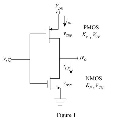
Consider the case when the input voltage is equal to zero.
The NMOS device is in the cutoff region the drain current of the transistor is zero and when the PMOS transistor is in the non-saturation region its drain current is also zero.
Consider the case when
The PMOS transistor in the Non-saturation and the NMOS just started to conduct and then enter in the saturation mode.
The expression for the drain current of the NMOS transistor is given by,
The expression for the drain current of the PMOS transistor is given by,
The CMOS drain current is due to the drain current of the NMOS alone and is given by,
Substitute
Substitute
The tale to determine the value of the output current for the different value of the output voltage is shown below.
The required table is shown in Table 1
Table 1
Consider the case when the input voltage is
The expression for the drain current of the PMOS in saturation is given by,
The expression for the drain current of the NMOS in non-saturation is given by,
The CMOS current depends only on the current through the drain current of the PMOS and is given by,
Substitute
Substitute
The table for the output current for the different values of the input voltage is shown below.
The required table is shown in Table 2
Table 2
Consider the case when the input voltage is given by,
For the above case the NMOS is in non-saturation region and the drain current is zero. The PMOS is in cut off and the drain current zero as the circuit is open.
The drain current when the input voltage is zero and the circuit is opened is given by,
The plot for the CMOS drain current against the input voltage from the values of table 1 and table 2 is shown below.
The required plot is shown in Figure 2
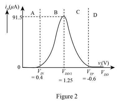
Conclusion:
Therefore, the required plot is shown in Figure 2.
(b)
To plot: The current in the transistor as a function fo the input voltage.
(b)
Answer to Problem 16.36P
The required plot is shown in Figure 3
Explanation of Solution
Calculation:
Consider the case when the voltage
Consider the input voltage as
Consider the case when the input voltage is
The expression for the drain current of the NMOS is given by,
The expression for the drain current of the PMOS transistor is given by,
The CMOS drain current is due to the drain current of the NMOS alone and is given by,
Substitute
Substitute
The table for the output current for the different values of the input voltage is shown below.
The required table is shown in Table 3
Table 3
Consider the case when the input voltage
The PMOS transistor is in the non-saturation and the NMOS just beings to conduct and then goes to saturation.
The expression for the drain current of the NMOS is given by,
The expression for the drain current of the PMOS transistor is given by,
The CMOS drain current is due to the drain current of the PMOS alone and is given by,
Substitute
Substitute
The table for the output current for the different values of the input voltage is shown below.
The required table is shown in Table 4
Table 4
Consider the case when the input voltage is
The plot between the drain current and the input voltage from table 3 and table 4 is shown below.
The required plot is shown in Figure 3
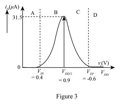
Conclusion:
Therefore, the required plot is shown in Figure 3
Want to see more full solutions like this?
Chapter 16 Solutions
Microelectronics: Circuit Analysis and Design


- Please answer ASAP and I'll give an upvote. Thanks. Consider the transistor inverter driving a DC motor modelled as a 10mH inductor shown on the right. The transistor has the following parameters: β=200, VBE,ON=0.65V and VCE,SAT=0.3V. The input voltage vi=5V for t<0s. Assume the transistor is in forward active mode. The input voltage remains at 0V for a very long time. Find iL(∞) and v0(∞).arrow_forwardA two-stage inverter is shown in this figure. Vs=50 V. v=110V2 sin 100 nt. The average voltage of C is set to be 200 V.1=2 A. The bipolar modulation scheme is applied on the inverter and the power factor of the inverter is set to be 1. Consider the two-stage inverter is lossless, Calculate the current of L. il (ii) Assume the voltage of Cr is a constant DC voltage of 200 V. Calculate the instantaneous duty ratio of the inverter. din if C = 75 HF, calculate the highest and lowest voltage of Cr.arrow_forwardDesign a depletion-load gate that implements thelogic function Y = A(B + CD) + E, based on thereference inverter design . (b) Redesign the W/L ratios of this gate to account for body effect and differences in values of VDS for thevarious transistorsarrow_forward
- Design an asymmetrical inverter to meet the delay of 250 ps for a load capacitance of 120 fF. Use VDD =1.5V, VTN =0.50 V, and VTP =−0.50 V. with (W/L)P = (W/L)N .arrow_forwardDefinition of the followingconcepts: LIDSTCNOCTString inverter Central inverter,Microinverter, MPPT - Difference between nema and iparrow_forwardThe drawing below shows a circuit with gates, the dimensions of which need to be selected in order to minimize the delay on the given path. The gates are scaled to a reference inverter with dimensions P/N = 3/1 and an input capacitance of 4C. The maximum input capacitance of the circuit is 8C. Calculate the dimensions of the P and N gate transistors on the schematic. Calculate the delay of the path assuming τ = 3RC = 200 ps.arrow_forward
- What factors contribute to the overall system efficiency of a solar pv system (that is system efficiency = system output/solar radiation reaching panels)? List all that apply. -panel efficiency -capacity factor -angle of incidence -inverter efficiency -derating factors (dirt, temperature)arrow_forward1. Draw the transistor level Diagram for the expression Y = (A+B) C+CD using CMOS technology. Also sketch the stick diagram. 2. Describe the read and write operation of a 6T SRAM cell with necessary figures.arrow_forwardThe single-phase half-bridge inverter has a resistive load of R = 2.4Ω and the DCinput voltage is 48V. Determine:1- the rms output voltage at the fundamental frequency2- fundamental displacement factor .3- fundamental power , drown from each source .4- fundamental load power .5- total power drown from each source .6- total load power .arrow_forward
- Draw the schematic of a three-input NAND gate. What are the W/L ratios for thetransistors based?arrow_forward'Home work (4) If the bridge inverter is loaded by an R-L laod with R=20 ©, L=30 mH. The inverter frequency, f,=50 Hz and the de input voltage, Vs=200 V. (@) Express the instantaneous load current in fourrier series. (b) Caleulate : i The rms load current at the fundamental frequency fi il The THD of the load current. iii. The power obserbed by the load (Po) and the fundamental power (Pol). Draw the waveform of the fundamental load current and show the intervals of transistors and diodes conduction.arrow_forwardUsing MOSFET design your own circuit such that it works as an inverter. (Hint: When input = high the output = low and vice versa) NOTE: DRAW USING SOME KIND OF CICUIT SOFTWARE(CIRCUIT WIZARD.LIVE WIRE or Any other online software) Hand made not accepted pleasearrow_forward
 Introductory Circuit Analysis (13th Edition)Electrical EngineeringISBN:9780133923605Author:Robert L. BoylestadPublisher:PEARSON
 Delmar's Standard Textbook Of ElectricityElectrical EngineeringISBN:9781337900348Author:Stephen L. HermanPublisher:Cengage Learning
 Programmable Logic ControllersElectrical EngineeringISBN:9780073373843Author:Frank D. PetruzellaPublisher:McGraw-Hill Education
 Fundamentals of Electric CircuitsElectrical EngineeringISBN:9780078028229Author:Charles K Alexander, Matthew SadikuPublisher:McGraw-Hill Education
 Electric Circuits. (11th Edition)Electrical EngineeringISBN:9780134746968Author:James W. Nilsson, Susan RiedelPublisher:PEARSON
 Engineering ElectromagneticsElectrical EngineeringISBN:9780078028151Author:Hayt, William H. (william Hart), Jr, BUCK, John A.Publisher:Mcgraw-hill Education,