
Concept explainers
Videos
Consider the circuit in Figure P2.62. The output of a diode AND logic gate is connected to the input of a second diode AND logic gate. Assume
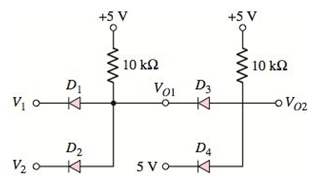
Figure P2.62
(a)
Values of output voltages
Answer to Problem 2.62P
The values of output voltages are
The values of output voltages are
The values of output voltages are
Explanation of Solution
Given:
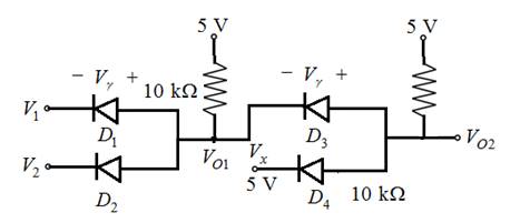
The given circuit is shown below.
Voltages given:
Calculation:
(i) Assume voltage
The entire circuit can be divided into two parts.
Now considering the first part,
On considering the connection of Diodes it is known that diodes are connected in reverse bias.
So, taking considerations from the first part, it is concluded that the output,
Hence, if the inputs of circuit are
Similarly, if the inputs of circuit are
Similarly, if the inputs of circuit are
Similarly, if the inputs of circuit are
Let’s make the truth table for
Table 1
| 0 0 5 5 | 0 5 0 | 0 0 0 5 |
On considering, the Boolean expression for
Now, taking considerations from the second part, as diodes are connected in reverse bias it is concluded that if any one of the inputs,
So the expression for the output voltage
Now for the given inputs
The diodes
Hence, from the expression for ideal diode output voltages are
(ii) Let’s assume voltage
The entire circuit can be divided into two parts.
Now considering the first part,
On considering the connection of Diodes it is known that diodes are connected in reverse bias.
So, taking considerations from the first part, it is concluded that the output,
Hence, if the inputs of circuit are
Similarly, if the inputs of circuit are
Similarly, if the inputs of circuit are
Similarly, if the inputs of circuit are
Let’s make the truth table for
Table 1
| 0 0 5 | 0 5 0 5 | 0 0 0 5 |
On considering, the Boolean expression for
Now, taking considerations from the second part, as diodes are connected in reverse bias it is concluded that if any one of the inputs,
So the expression for the output voltage
Now for the given inputs,
The diodes
Calculating the value of output voltage,
Calculating the value of output voltage,
Hence, output voltages are
(iii) Let’s assume voltage
The entire circuit can be divided into two parts.
Now considering the first part,
On considering the connection of Diodes it is known that diodes are connected in reverse bias.
So, taking considerations from the first part, it is concluded that the output,
Hence, if the inputs of circuit are
Similarly, if the inputs of circuit are
Similarly, if the inputs of circuit are
Similarly, if the inputs of circuit are
Let’s make the truth table for
Table 1
| 0 0 5 5 | 0 5 0 5 | 0 0 0 5 |
On considering, the Boolean expression for
Now, taking considerations from the second part, as diodes are connected in reverse bias it is concluded that if any one of the inputs,
So the expression for the output voltage
Now for the given inputs
The diodes
Calculating the value of output voltage,
Calculating the value of output voltage,
Hence, output voltages are
Therefore, in their LOW states the value of
(b)
Relative values of VO1 and VO2 in their “low” state
Answer to Problem 2.62P
Logic “0” signal degrades as it goes through additional logic gates.
Explanation of Solution
Given:
The given circuit is shown below.

Circuit diagram:

Logic “0” signal degrades as it goes through additional logic gates.
The diodes
Calculating the value of output voltage,
Calculating the value of output voltage,
Hence, output voltages are
Want to see more full solutions like this?
Chapter 2 Solutions
Microelectronics: Circuit Analysis and Design


- The temperature dependence of resistance is also quantified by the relation R2=R1[ 1+(T2T1) ] where R1 and R2 are the resistances at temperatures T1 and T2, respectively, and is known as the temperature coefficient of resistance. If a copper wire has a resistance of 55 at 20C, find the maximum permissible operating temperature of the wire if its resistance is to increase by at most 20. Take the temperature coefficient at 20C to be =0.00382.arrow_forwardConsider the full-wave rectifier circuit shown below, where• vS(t) is a sinusoidal signal with a peak value (Vs = 5 V).• Diodes are modelled using constant voltage model with VDO = 0.7 V• The ac line voltage has an rms value of 120 V and a frequency (f) = 60 Hza) Calculate the transformer turns ratio. b) Plot in the same graph signal vS(t) and the output signal vO(t) versus time (t) (show all details including amplitudes, time instances, etc.) c) Calculate the rms value of the output signal vO(t). (hint: sin2(x) = 0.5(1- cos(2x))) d) If a capacitor C=3.58 F is connected across R = 10 k, repeat (b) in a new grapharrow_forwardA number of diodes rated at 1620 V each are to be connected in series in a rectifier circuit with a maximum voltage of 3000V. A de-rating factor of 15% is recommended. The maximum difference in leakage current of the diodes is given as 10mA , and the maximum difference in stored charge is 20µC. Calculate, 1) the number of diodes that must be used, 2) a suitable component value for the static equalization circuit; 3) a suitable component value for the dynamic equalization circuit.arrow_forward
- In a 1-phase full wave bridge rectifier with Vs = Vm sin ωt, with R load & ideal diodes. The expression for the average value of the output voltage is 2Vm/π Select one: True Falsearrow_forwardDesign Half-wave Rectifier Circuit to provide an output of 100 VDC. Then calculate its transformer peak voltage rating, the diode PIV rating, and the transformer turns ratio, if the power is taken from the 220V line AC supplyarrow_forwardAssume that an input signal is applied to the circuit given above, as shown in the figure next to it. Accordingly, answer the following questions. The diodes used are silicon diodes, their operating voltages are 0.7 volts, and can be omitted because their resistance is very small. a) Write the name of this circuit, thinking about which circuit we do in the courses is equivalent to the purpose. b) What are the diodes/diodes that are active in a positive half-loop? Please type. c) What are the diodes/diodes active in the negative half-loop? Please type. d) Calculate ? ?−???( ?? ) for this circuit.arrow_forward
- Redraw the circuit and determine the value of ID and VO for the diode configurationshown in Figure Q2a.arrow_forwardWhat is the condition to obtain the maximum efficiency of a Rectifier? Neglecting the value of total resistance Neglecting the value of transformer resistance Neglecting the value of diode resistance Neglecting the value of load resistancearrow_forwardDesign a center-tapped full-wave Rectifier Circuit to provide an output of 100 VDC. Then calculate its transformer peak voltage rating, the diode PIV rating, and the transformer turns ratio, if the power is taken from the 220V line AC supplyarrow_forward
- Derive the current equations for the circuit shown below, using the labels as shown.Note that rz here is a model of the parasitic imperfection of the Zener diode.a) IL = ?b) II = ?c) IZ = ?d) What impact does rz have on VL?arrow_forwardFigure shows an AC source G having an effective voltage of 240 V, 60 Hz is connected to a single-phase full-wave rectifier. The resistance for R is 53 Ω and ripple-to-ripple current is 15%.Determine the DC voltage and DC current across the resistor. Hence, determine the power absorbed by the load. Assuming all diodes are ideal.arrow_forwardHow is Zener diode connected into a circuit? What determines the voltage at which a Zener diode break down? What considerations go into determining the power dissipation rating of a Zener diode? Draw a label the schematic symbol used to represent a Zener diode What determines the maximum Zener current of a Zener diode? What is the difference between the maximum Zener current and the reverse current for a Zener diode? What does a positive Zener voltage temperature coefficient signify? What does a negative Zener voltage temperature coefficient signify? How can a Zener diode be temperature compensated?arrow_forward
 Power System Analysis and Design (MindTap Course ...Electrical EngineeringISBN:9781305632134Author:J. Duncan Glover, Thomas Overbye, Mulukutla S. SarmaPublisher:Cengage Learning