
Microelectronics: Circuit Analysis and Design
4th Edition
ISBN: 9780073380643
Author: Donald A. Neamen
Publisher: McGraw-Hill Companies, The
expand_more
expand_more
format_list_bulleted
Concept explainers
Videos
Textbook Question
Chapter 2, Problem 2.56P
If
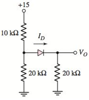
Figure P2.56
Expert Solution & Answer
Want to see the full answer?
Check out a sample textbook solution
Students have asked these similar questions
accepting that D1 and D2 diodes have the same properties in the circuit given in the figurea) output voltage, b) current flowing through the resistor,c) current flowing from diodes calculate.
⦁ Consider the below zener diode circuit and find the values of , , , . Use the constant voltage drop model which is shown is Figure 2. Show your solution steps clearly and explain them. The answers without solution steps will not be graded. Also, state your results in the sections below the circuits. ( = 0.1 )
For the circuit shown in Figure 2-a, plot the output voltage across the resistance R, using the diode characteristic presented in Figure 2-b. Assume the input AC voltage supply given by
Vs = 1. sin(2pifot). Where fo = 100 Hz.
In addition, could you suggest a method on how to keep the output voltage more constant.
Chapter 2 Solutions
Microelectronics: Circuit Analysis and Design
Ch. 2 - Repeat Example 2.1 if the input voltage is...Ch. 2 - Consider the bridge circuit shown in Figure 2.6(a)...Ch. 2 - Assume the input signal to a rectifier circuit has...Ch. 2 - The input voltage to the halfwave rectifier in...Ch. 2 - Consider the circuit in Figure 2.4. The input...Ch. 2 - The circuit in Figure 2.5(a) is used to rectify a...Ch. 2 - The secondary transformer voltage of the rectifier...Ch. 2 - Determine the fraction (percent) of the cycle that...Ch. 2 - The Zener diode regulator circuit shown in Figure...Ch. 2 - Repeat Example 2.6 for rz=4 . Assume all other...
Ch. 2 - Consider the circuit shown in Figure 2.19. Let...Ch. 2 - Suppose the currentlimiting resistor in Example...Ch. 2 - Suppose the power supply voltage in the circuit...Ch. 2 - Design a parallelbased clipper that will yield the...Ch. 2 - Sketch the steadystate output voltage for the...Ch. 2 - Consider the circuit in Figure 2.23(a). Let R1=5k...Ch. 2 - Determine the steadystate output voltage O for the...Ch. 2 - Design a parallelbased clipper circuit that will...Ch. 2 - Consider the circuit shown in Figure 2.38, in...Ch. 2 - Consider the circuit shown in Figure 2.39. The...Ch. 2 - Repeat Example 2.11 for the case when R1=8k ,...Ch. 2 - The cutin voltage of each diode in the circuit...Ch. 2 - Prob. 2.12TYUCh. 2 - Consider the OR logic circuit shown in Figure...Ch. 2 - Consider the AND logic circuit shown in Figure...Ch. 2 - (a) Photons with an energy of hv=2eV are incident...Ch. 2 - Determine the value of resistance R required to...Ch. 2 - What characteristic of a diode is used in the...Ch. 2 - Prob. 2RQCh. 2 - Describe a simple fullwave diode rectifier circuit...Ch. 2 - Prob. 4RQCh. 2 - Prob. 5RQCh. 2 - Describe a simple Zener diode voltage reference...Ch. 2 - What effect does the Zener diode resistance have...Ch. 2 - What are the general characteristics of diode...Ch. 2 - Describe a simple diode clipper circuit that...Ch. 2 - Prob. 10RQCh. 2 - What one circuit element, besides a diode, is...Ch. 2 - Prob. 12RQCh. 2 - Describe a diode OR logic circuit. Compare a logic...Ch. 2 - Describe a diode AND logic circuit. Compare a...Ch. 2 - Describe a simple circuit that can be used to turn...Ch. 2 - Consider the circuit shown in Figure P2.1. Let...Ch. 2 - For the circuit shown in Figure P2.1, show that...Ch. 2 - A halfwave rectifier such as shown in Figure...Ch. 2 - Consider the battery charging circuit shown in...Ch. 2 - Figure P2.5 shows a simple fullwave battery...Ch. 2 - The fullwave rectifier circuit shown in Figure...Ch. 2 - The input signal voltage to the fullwave rectifier...Ch. 2 - The output resistance of the fullwave rectifier in...Ch. 2 - Repeat Problem 2.8 for the halfwave rectifier in...Ch. 2 - Consider the halfwave rectifier circuit shown in...Ch. 2 - The parameters of the halfwave rectifier circuit...Ch. 2 - The fullwave rectifier circuit shown in Figure...Ch. 2 - Consider the fullwave rectifier circuit in Figure...Ch. 2 - The circuit in Figure P2.14 is a complementary...Ch. 2 - Prob. 2.15PCh. 2 - A fullwave rectifier is to be designed using the...Ch. 2 - Prob. 2.17PCh. 2 - (a) Sketch o versus time for the circuit in Figure...Ch. 2 - Consider the circuit shown in Figure P2.19. The...Ch. 2 - Consider the Zener diode circuit shown in Figure...Ch. 2 - Consider the Zener diode circuit shown in Figure...Ch. 2 - In the voltage regulator circuit in Figure P2.21,...Ch. 2 - A Zener diode is connected in a voltage regulator...Ch. 2 - Consider the Zener diode circuit in Figure 2.19 in...Ch. 2 - Design a voltage regulator circuit such as shown...Ch. 2 - The percent regulation of the Zener diode...Ch. 2 - A voltage regulator is to have a nominal output...Ch. 2 - Consider the circuit in Figure P2.28. Let V=0 ....Ch. 2 - The secondary voltage in the circuit in Figure...Ch. 2 - The parameters in the circuit shown in Figure...Ch. 2 - Consider the circuit in Figure P2.31. Let V=0 (a)...Ch. 2 - Prob. 2.32PCh. 2 - Each diode cutin voltage is 0.7 V for the circuits...Ch. 2 - The diode in the circuit of Figure P2.34(a) has...Ch. 2 - Consider the circuits shown in Figure P2.35. Each...Ch. 2 - Plot O for each circuit in Figure P2.36 for the...Ch. 2 - Consider the parallel clipper circuit in Figure...Ch. 2 - A car’s radio may be subjected to voltage spikes...Ch. 2 - Sketch the steadystate output voltage O versus...Ch. 2 - Prob. D2.40PCh. 2 - Design a diode clamper to generate a steadystate...Ch. 2 - For the circuit in Figure P2.39(b), let V=0 and...Ch. 2 - Repeat Problem 2.42 for the circuit in Figure...Ch. 2 - The diodes in the circuit in Figure P2.44 have...Ch. 2 - In the circuit in Figure P2.45 the diodes have the...Ch. 2 - The diodes in the circuit in Figure P2.46 have the...Ch. 2 - Consider the circuit shown in Figure P2.47. Assume...Ch. 2 - The diode cutin voltage for each diode in the...Ch. 2 - Consider the circuit in Figure P2.49. Each diode...Ch. 2 - Assume V=0.7V for each diode in the circuit in...Ch. 2 - The cutin voltage of each diode in the circuit...Ch. 2 - Let V=0.7V for each diode in the circuit in Figure...Ch. 2 - For the circuit shown in Figure P2.54, let V=0.7V...Ch. 2 - Assume each diode cutin voltage is V=0.7V for the...Ch. 2 - If V=0.7V for the diode in the circuit in Figure...Ch. 2 - Let V=0.7V for the diode in the circuit in Figure...Ch. 2 - Each diode cutin voltage in the circuit in Figure...Ch. 2 - Let V=0.7V for each diode in the circuit shown in...Ch. 2 - Consider the circuit in Figure P2.61. The output...Ch. 2 - Consider the circuit in Figure P2.62. The output...Ch. 2 - Prob. 2.63PCh. 2 - Consider the circuit shown in Figure P2.64. The...Ch. 2 - The lightemitting diode in the circuit shown in...Ch. 2 - The parameters of D1 and D2 in the circuit shown...Ch. 2 - If the resistor in Example 2.12 is R=2 and the...Ch. 2 - Consider the photodiode circuit shown in Figure...Ch. 2 - Consider the fullwave bridge rectifier circuit....Ch. 2 - Design a simple dc voltage source using a...Ch. 2 - A clipper is to be designed such that O=2.5V for...Ch. 2 - Design a circuit to provide the voltage transfer...
Knowledge Booster


Learn more about
Need a deep-dive on the concept behind this application? Look no further. Learn more about this topic, electrical-engineering and related others by exploring similar questions and additional content below.Similar questions
- Q2 (b) Multiple diodes circuit is given in Figure (i) Identify the condition for Si and Ge diodes. (ii) Determine the current flowing into Si and Ge diodes. (iii) Calculate the output voltage, Voarrow_forwardConsider a Zener diode in the figure given below where, V1 = 30 V. Determine the Zener current IZ if RZ = 100 Ω.arrow_forward2-2VOLTAGE-CURRENT CHARACTERISTICOF A DIODE 1.Explain how to generate the forward-bias portion of the characteristic curve. 2.What would cause the barrier potential of a silicon diode to decrease from 0.7 V to 0.6 V?arrow_forward
- Determine Q-point for the diodes in the circuit given below using the ideal diode model where, R1 = 12.2 kΩ, R2 = 16 kΩ, and R3 = 14 kΩ. (Note: Label the diodes from left to right.)arrow_forwardIn one graph, sketch the I-V curve for the forward bias. Forward Bias of PN Junction Diode:1. The Cut in Voltage or Knee Voltage of 1N4148 is _____________Volts.2. The Static Forward resistance of 1N4148 is __________________ .arrow_forwardIn the circuit shown in Figure 2–52 (p. 97), the Zener diode has a reverse breakdown voltage of 12V. RS = 50 Ohms, VS = 20V, and RL can vary from 100 Ohms to 200 Ohms. Assuming that the Zener diode remains in breakdown, find: (a) the minimum and maximum current in the Zener diode; (b) the minimum and maximum power dissipated in the diode; and (c) the minimum rated power dissipation that RS should have.arrow_forward
- Calculate diode forward current IF, diode voltage VF, and voltage drop across series resistor for three diode models (ideal, practical and complex). Assume diode forward resistance (dynamic resistance) r’d = 25Ω. Reverse leakage current IR = 75A with series resistance of RL = 100kΩ in reverse bias. Draw equivalent circuit diagrams of each model separately and plot corresponding I/V characteristics for each model.arrow_forwardDraw sketches to illustrate the behaviour of the following: i. Reverse Biased Zener Diode ii. Ideal Diode iii. Forward Biased Practical Diode iv. Equivalent circuit of a simple diode circuit v. Practical Diode at Average AC Resistance Levelarrow_forwardIn a 1-phase full wave bridge rectifier with Vs = Vm sin ωt, with R load & ideal diodes. The expression for the average value of the output voltage is 2Vm/π Select one: True Falsearrow_forward
- Q2:- Find the level of Vo for each circuit shown in the Figure below. Also, determine the status of each diode; if it is forward or reverses biasing. Assume all diodes are silicone with 0.7v drop.arrow_forwardCalculate diode forward current IF, diode voltage VF, and voltage drop across series resistor for three diode models (ideal, practical and complex).Assume diode forward resistance (dynamic resistance) r’d = 25Ω. Reverse leakage current IR = 75 nanoA with series resistance of RL = 100kΩ in reverse bias. Draw equivalent circuit diagrams of each model separately and plot corresponding I/V characteristics for each model.arrow_forwardQuestion: The circuit in Figure P2.14 is a complementary output rectifier. If vs = 26 sin [2?(60)t]V, sketc... The circuit in Figure is a complementary output rectifier. If vs = 26√2sin[120πt]V,sketch the output waveforms vo+ and vo? assumingV? =0.6V for each diode. And explain the operation of the circuit.arrow_forward
arrow_back_ios
SEE MORE QUESTIONS
arrow_forward_ios
Recommended textbooks for you

Diodes Explained - The basics how diodes work working principle pn junction; Author: The Engineering Mindset;https://www.youtube.com/watch?v=Fwj_d3uO5g8;License: Standard Youtube License