
Microelectronics: Circuit Analysis and Design
4th Edition
ISBN: 9780073380643
Author: Donald A. Neamen
Publisher: McGraw-Hill Companies, The
expand_more
expand_more
format_list_bulleted
Concept explainers
Videos
Textbook Question
Chapter 2, Problem 2.7EP
Design a parallel−based clipper that will yield the voltage transfer function shown in Figure 2.24. Assume diode cut−in voltages of
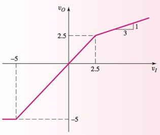
Figure 2.24 Figure for Exercise Ex 2.7
Expert Solution & Answer
Want to see the full answer?
Check out a sample textbook solution
Students have asked these similar questions
For the circuit shown in Figure 2-a, plot the output voltage across the resistance R, using the diode characteristic presented in Figure 2-b. Assume the input AC voltage supply given by
Vs = 1. sin(2pifot). Where fo = 100 Hz.
In addition, could you suggest a method on how to keep the output voltage more constant.
For the values of R1=230, R2=230, R3=400, Vs=15. If the real diode (offset voltage=0.7V) were conduxting, then the value of voltage source Vb should be?
solve correct or will dislike
diode zener
a, DESIGN THE NETWORK IN THE FIGURE, TO KEEP, "VL" at 12 V for a variation in load (IL) from 0 to 200 mA, DETERMINE "Rs" and "Vz"
b. determine "P2min" for the Zener diode from section a
Chapter 2 Solutions
Microelectronics: Circuit Analysis and Design
Ch. 2 - Repeat Example 2.1 if the input voltage is...Ch. 2 - Consider the bridge circuit shown in Figure 2.6(a)...Ch. 2 - Assume the input signal to a rectifier circuit has...Ch. 2 - The input voltage to the halfwave rectifier in...Ch. 2 - Consider the circuit in Figure 2.4. The input...Ch. 2 - The circuit in Figure 2.5(a) is used to rectify a...Ch. 2 - The secondary transformer voltage of the rectifier...Ch. 2 - Determine the fraction (percent) of the cycle that...Ch. 2 - The Zener diode regulator circuit shown in Figure...Ch. 2 - Repeat Example 2.6 for rz=4 . Assume all other...
Ch. 2 - Consider the circuit shown in Figure 2.19. Let...Ch. 2 - Suppose the currentlimiting resistor in Example...Ch. 2 - Suppose the power supply voltage in the circuit...Ch. 2 - Design a parallelbased clipper that will yield the...Ch. 2 - Sketch the steadystate output voltage for the...Ch. 2 - Consider the circuit in Figure 2.23(a). Let R1=5k...Ch. 2 - Determine the steadystate output voltage O for the...Ch. 2 - Design a parallelbased clipper circuit that will...Ch. 2 - Consider the circuit shown in Figure 2.38, in...Ch. 2 - Consider the circuit shown in Figure 2.39. The...Ch. 2 - Repeat Example 2.11 for the case when R1=8k ,...Ch. 2 - The cutin voltage of each diode in the circuit...Ch. 2 - Prob. 2.12TYUCh. 2 - Consider the OR logic circuit shown in Figure...Ch. 2 - Consider the AND logic circuit shown in Figure...Ch. 2 - (a) Photons with an energy of hv=2eV are incident...Ch. 2 - Determine the value of resistance R required to...Ch. 2 - What characteristic of a diode is used in the...Ch. 2 - Prob. 2RQCh. 2 - Describe a simple fullwave diode rectifier circuit...Ch. 2 - Prob. 4RQCh. 2 - Prob. 5RQCh. 2 - Describe a simple Zener diode voltage reference...Ch. 2 - What effect does the Zener diode resistance have...Ch. 2 - What are the general characteristics of diode...Ch. 2 - Describe a simple diode clipper circuit that...Ch. 2 - Prob. 10RQCh. 2 - What one circuit element, besides a diode, is...Ch. 2 - Prob. 12RQCh. 2 - Describe a diode OR logic circuit. Compare a logic...Ch. 2 - Describe a diode AND logic circuit. Compare a...Ch. 2 - Describe a simple circuit that can be used to turn...Ch. 2 - Consider the circuit shown in Figure P2.1. Let...Ch. 2 - For the circuit shown in Figure P2.1, show that...Ch. 2 - A halfwave rectifier such as shown in Figure...Ch. 2 - Consider the battery charging circuit shown in...Ch. 2 - Figure P2.5 shows a simple fullwave battery...Ch. 2 - The fullwave rectifier circuit shown in Figure...Ch. 2 - The input signal voltage to the fullwave rectifier...Ch. 2 - The output resistance of the fullwave rectifier in...Ch. 2 - Repeat Problem 2.8 for the halfwave rectifier in...Ch. 2 - Consider the halfwave rectifier circuit shown in...Ch. 2 - The parameters of the halfwave rectifier circuit...Ch. 2 - The fullwave rectifier circuit shown in Figure...Ch. 2 - Consider the fullwave rectifier circuit in Figure...Ch. 2 - The circuit in Figure P2.14 is a complementary...Ch. 2 - Prob. 2.15PCh. 2 - A fullwave rectifier is to be designed using the...Ch. 2 - Prob. 2.17PCh. 2 - (a) Sketch o versus time for the circuit in Figure...Ch. 2 - Consider the circuit shown in Figure P2.19. The...Ch. 2 - Consider the Zener diode circuit shown in Figure...Ch. 2 - Consider the Zener diode circuit shown in Figure...Ch. 2 - In the voltage regulator circuit in Figure P2.21,...Ch. 2 - A Zener diode is connected in a voltage regulator...Ch. 2 - Consider the Zener diode circuit in Figure 2.19 in...Ch. 2 - Design a voltage regulator circuit such as shown...Ch. 2 - The percent regulation of the Zener diode...Ch. 2 - A voltage regulator is to have a nominal output...Ch. 2 - Consider the circuit in Figure P2.28. Let V=0 ....Ch. 2 - The secondary voltage in the circuit in Figure...Ch. 2 - The parameters in the circuit shown in Figure...Ch. 2 - Consider the circuit in Figure P2.31. Let V=0 (a)...Ch. 2 - Prob. 2.32PCh. 2 - Each diode cutin voltage is 0.7 V for the circuits...Ch. 2 - The diode in the circuit of Figure P2.34(a) has...Ch. 2 - Consider the circuits shown in Figure P2.35. Each...Ch. 2 - Plot O for each circuit in Figure P2.36 for the...Ch. 2 - Consider the parallel clipper circuit in Figure...Ch. 2 - A car’s radio may be subjected to voltage spikes...Ch. 2 - Sketch the steadystate output voltage O versus...Ch. 2 - Prob. D2.40PCh. 2 - Design a diode clamper to generate a steadystate...Ch. 2 - For the circuit in Figure P2.39(b), let V=0 and...Ch. 2 - Repeat Problem 2.42 for the circuit in Figure...Ch. 2 - The diodes in the circuit in Figure P2.44 have...Ch. 2 - In the circuit in Figure P2.45 the diodes have the...Ch. 2 - The diodes in the circuit in Figure P2.46 have the...Ch. 2 - Consider the circuit shown in Figure P2.47. Assume...Ch. 2 - The diode cutin voltage for each diode in the...Ch. 2 - Consider the circuit in Figure P2.49. Each diode...Ch. 2 - Assume V=0.7V for each diode in the circuit in...Ch. 2 - The cutin voltage of each diode in the circuit...Ch. 2 - Let V=0.7V for each diode in the circuit in Figure...Ch. 2 - For the circuit shown in Figure P2.54, let V=0.7V...Ch. 2 - Assume each diode cutin voltage is V=0.7V for the...Ch. 2 - If V=0.7V for the diode in the circuit in Figure...Ch. 2 - Let V=0.7V for the diode in the circuit in Figure...Ch. 2 - Each diode cutin voltage in the circuit in Figure...Ch. 2 - Let V=0.7V for each diode in the circuit shown in...Ch. 2 - Consider the circuit in Figure P2.61. The output...Ch. 2 - Consider the circuit in Figure P2.62. The output...Ch. 2 - Prob. 2.63PCh. 2 - Consider the circuit shown in Figure P2.64. The...Ch. 2 - The lightemitting diode in the circuit shown in...Ch. 2 - The parameters of D1 and D2 in the circuit shown...Ch. 2 - If the resistor in Example 2.12 is R=2 and the...Ch. 2 - Consider the photodiode circuit shown in Figure...Ch. 2 - Consider the fullwave bridge rectifier circuit....Ch. 2 - Design a simple dc voltage source using a...Ch. 2 - A clipper is to be designed such that O=2.5V for...Ch. 2 - Design a circuit to provide the voltage transfer...
Knowledge Booster


Learn more about
Need a deep-dive on the concept behind this application? Look no further. Learn more about this topic, electrical-engineering and related others by exploring similar questions and additional content below.Similar questions
- In the circuit shown in Figure 2–52 (p. 97), the Zener diode has a reverse breakdown voltage of 12V. RS = 50 Ohms, VS = 20V, and RL can vary from 100 Ohms to 200 Ohms. Assuming that the Zener diode remains in breakdown, find: (a) the minimum and maximum current in the Zener diode; (b) the minimum and maximum power dissipated in the diode; and (c) the minimum rated power dissipation that RS should have.arrow_forwardConsider the circuit in Figure 2–75 .(a) What type of circuit is this?(b) What is the total peak secondary voltage?(c) Find the peak voltage across each half of the secondary.(d) Sketch the voltage waveform across RL.(e) What is the peak current through each diode?(f) What is the PIV for each diode?arrow_forwarda. Using standard resistor values, what value of R1 is needed to achieve 1.18V ±0.01V at Vout? b. Using the R1 value chosen in (a) part, what happens to the voltage Vout when a load resistance of 10K is added (between Vout and ground). c. What is the minimum value of load resistance required for correct operation Zener diode is used in place of si diode. Or you can assume zener current according to requirement Answer it i will ratearrow_forward
- In one graph, sketch the I-V curve for the forward bias. Forward Bias of PN Junction Diode:1. The Cut in Voltage or Knee Voltage of 1N4148 is _____________Volts.2. The Static Forward resistance of 1N4148 is __________________ .arrow_forward2-2VOLTAGE-CURRENT CHARACTERISTICOF A DIODE 1.Explain how to generate the forward-bias portion of the characteristic curve. 2.What would cause the barrier potential of a silicon diode to decrease from 0.7 V to 0.6 V?arrow_forwardCompute the value of DC resistance and AC resistance of a Germanium junction diode at 250C with reverse saturation current, I0 = 25µA and at an applied voltage of 0.2V across the diode.arrow_forward
- Calculate diode forward current IF, diode voltage VF, and voltage drop across series resistor for three diode models (ideal, practical and complex).Assume diode forward resistance (dynamic resistance) r’d = 25Ω. Reverse leakage current IR = 75 nanoA with series resistance of RL = 100kΩ in reverse bias. Draw equivalent circuit diagrams of each model separately and plot corresponding I/V characteristics for each model.arrow_forwardCalculate diode forward current IF, diode voltage VF, and voltage drop across series resistor for three diode models (ideal, practical and complex). Assume diode forward resistance (dynamic resistance) r’d = 25Ω. Reverse leakage current IR = 75A with series resistance of RL = 100kΩ in reverse bias. Draw equivalent circuit diagrams of each model separately and plot corresponding I/V characteristics for each model.arrow_forwardIn a 1-phase full wave bridge rectifier with Vs = Vm sin ωt, with R load & ideal diodes. The expression for the average value of the output voltage is 2Vm/π Select one: True Falsearrow_forward
- Briefly discuss the difference between Diode Piecewise-linear model, Simplified model, and Ideal device/ equivalent circuit. Study the diode specification sheets of a 1N4001 and 1N5401 diodes provided by the manufacturer and compare their difference. Give typical application of each. Discuss briefly how to test junction diode.arrow_forwardsolve all on the keyboard or will dislike if need draw on paper no problem (a) Explain the following terms as they relate to semiconductor diodes: Avalanche effect, Depletion region, and Intrinsic semiconductor (b) With the aid of fully labeled Crystal Lattice Structure diagram (s), explain how P-type material of a semiconductor is formed. (c) Draw a diagram showing the volt-ampere characteristic of a Zener diode. Explain the difference between Zener breakdown and Avalanche breakdown mechanisms. (d) A bridge rectifier is supplied with 120Vrms sinusoidal signal. If each diode has a junction voltage of 0.7V, determine: The peak voltage at the output of the rectifier and A suitable peak inverse voltage rating of each diodearrow_forwardUsing constant-voltage diode model, where VDO = 0.5 V, plot vo versus vi. Make sure to show all steps, initial plots with dashed lines, final plot, amplitudes, slopes, intersection with axis, etc.arrow_forward
arrow_back_ios
SEE MORE QUESTIONS
arrow_forward_ios
Recommended textbooks for you

Diodes Explained - The basics how diodes work working principle pn junction; Author: The Engineering Mindset;https://www.youtube.com/watch?v=Fwj_d3uO5g8;License: Standard Youtube License