
Microelectronics: Circuit Analysis and Design
4th Edition
ISBN: 9780073380643
Author: Donald A. Neamen
Publisher: McGraw-Hill Companies, The
expand_more
expand_more
format_list_bulleted
Videos
Textbook Question
Chapter 2, Problem 2.12P
The full−wave rectifier circuit shown in Figure P2.12 has an input signal whose frequency is 60 Hz. The rms value of
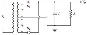
Figure P2.12
Expert Solution & Answer
Want to see the full answer?
Check out a sample textbook solution
Students have asked these similar questions
Consider the full-wave rectifier circuit shown below, where• vS(t) is a sinusoidal signal with a peak value (Vs = 5 V).• Diodes are modelled using constant voltage model with VDO = 0.7 V• The ac line voltage has an rms value of 120 V and a frequency (f) = 60 Hza) Calculate the transformer turns ratio.
b) Plot in the same graph signal vS(t) and the output signal vO(t) versus time (t) (show all details including amplitudes, time instances, etc.)
c) Calculate the rms value of the output signal vO(t). (hint: sin2(x) = 0.5(1- cos(2x)))
d) If a capacitor C=3.58 F is connected across R = 10 k, repeat (b) in a new graph
In a 1-phase full wave bridge rectifier with Vs = Vm sin ωt, with R load & ideal diodes. The expression for the average value of the output voltage is 2Vm/π
Select one:
True
False
(1) Sketch the circuit for an ac supply input to a full-wave diode rectifier with a resistive load and no smoothing capacitor.
(2).Sketch the ac supply voltage and the voltage across the resistive load in (question no 1)indicating the period of the resistive load voltage.
(3) For the circuit in (question no 1) calculate the average and rms voltages across the resistive load for an rms ac supply voltage of 115 V assuming no diode voltage.
Chapter 2 Solutions
Microelectronics: Circuit Analysis and Design
Ch. 2 - Repeat Example 2.1 if the input voltage is...Ch. 2 - Consider the bridge circuit shown in Figure 2.6(a)...Ch. 2 - Assume the input signal to a rectifier circuit has...Ch. 2 - The input voltage to the halfwave rectifier in...Ch. 2 - Consider the circuit in Figure 2.4. The input...Ch. 2 - The circuit in Figure 2.5(a) is used to rectify a...Ch. 2 - The secondary transformer voltage of the rectifier...Ch. 2 - Determine the fraction (percent) of the cycle that...Ch. 2 - The Zener diode regulator circuit shown in Figure...Ch. 2 - Repeat Example 2.6 for rz=4 . Assume all other...
Ch. 2 - Consider the circuit shown in Figure 2.19. Let...Ch. 2 - Suppose the currentlimiting resistor in Example...Ch. 2 - Suppose the power supply voltage in the circuit...Ch. 2 - Design a parallelbased clipper that will yield the...Ch. 2 - Sketch the steadystate output voltage for the...Ch. 2 - Consider the circuit in Figure 2.23(a). Let R1=5k...Ch. 2 - Determine the steadystate output voltage O for the...Ch. 2 - Design a parallelbased clipper circuit that will...Ch. 2 - Consider the circuit shown in Figure 2.38, in...Ch. 2 - Consider the circuit shown in Figure 2.39. The...Ch. 2 - Repeat Example 2.11 for the case when R1=8k ,...Ch. 2 - The cutin voltage of each diode in the circuit...Ch. 2 - Prob. 2.12TYUCh. 2 - Consider the OR logic circuit shown in Figure...Ch. 2 - Consider the AND logic circuit shown in Figure...Ch. 2 - (a) Photons with an energy of hv=2eV are incident...Ch. 2 - Determine the value of resistance R required to...Ch. 2 - What characteristic of a diode is used in the...Ch. 2 - Prob. 2RQCh. 2 - Describe a simple fullwave diode rectifier circuit...Ch. 2 - Prob. 4RQCh. 2 - Prob. 5RQCh. 2 - Describe a simple Zener diode voltage reference...Ch. 2 - What effect does the Zener diode resistance have...Ch. 2 - What are the general characteristics of diode...Ch. 2 - Describe a simple diode clipper circuit that...Ch. 2 - Prob. 10RQCh. 2 - What one circuit element, besides a diode, is...Ch. 2 - Prob. 12RQCh. 2 - Describe a diode OR logic circuit. Compare a logic...Ch. 2 - Describe a diode AND logic circuit. Compare a...Ch. 2 - Describe a simple circuit that can be used to turn...Ch. 2 - Consider the circuit shown in Figure P2.1. Let...Ch. 2 - For the circuit shown in Figure P2.1, show that...Ch. 2 - A halfwave rectifier such as shown in Figure...Ch. 2 - Consider the battery charging circuit shown in...Ch. 2 - Figure P2.5 shows a simple fullwave battery...Ch. 2 - The fullwave rectifier circuit shown in Figure...Ch. 2 - The input signal voltage to the fullwave rectifier...Ch. 2 - The output resistance of the fullwave rectifier in...Ch. 2 - Repeat Problem 2.8 for the halfwave rectifier in...Ch. 2 - Consider the halfwave rectifier circuit shown in...Ch. 2 - The parameters of the halfwave rectifier circuit...Ch. 2 - The fullwave rectifier circuit shown in Figure...Ch. 2 - Consider the fullwave rectifier circuit in Figure...Ch. 2 - The circuit in Figure P2.14 is a complementary...Ch. 2 - Prob. 2.15PCh. 2 - A fullwave rectifier is to be designed using the...Ch. 2 - Prob. 2.17PCh. 2 - (a) Sketch o versus time for the circuit in Figure...Ch. 2 - Consider the circuit shown in Figure P2.19. The...Ch. 2 - Consider the Zener diode circuit shown in Figure...Ch. 2 - Consider the Zener diode circuit shown in Figure...Ch. 2 - In the voltage regulator circuit in Figure P2.21,...Ch. 2 - A Zener diode is connected in a voltage regulator...Ch. 2 - Consider the Zener diode circuit in Figure 2.19 in...Ch. 2 - Design a voltage regulator circuit such as shown...Ch. 2 - The percent regulation of the Zener diode...Ch. 2 - A voltage regulator is to have a nominal output...Ch. 2 - Consider the circuit in Figure P2.28. Let V=0 ....Ch. 2 - The secondary voltage in the circuit in Figure...Ch. 2 - The parameters in the circuit shown in Figure...Ch. 2 - Consider the circuit in Figure P2.31. Let V=0 (a)...Ch. 2 - Prob. 2.32PCh. 2 - Each diode cutin voltage is 0.7 V for the circuits...Ch. 2 - The diode in the circuit of Figure P2.34(a) has...Ch. 2 - Consider the circuits shown in Figure P2.35. Each...Ch. 2 - Plot O for each circuit in Figure P2.36 for the...Ch. 2 - Consider the parallel clipper circuit in Figure...Ch. 2 - A car’s radio may be subjected to voltage spikes...Ch. 2 - Sketch the steadystate output voltage O versus...Ch. 2 - Prob. D2.40PCh. 2 - Design a diode clamper to generate a steadystate...Ch. 2 - For the circuit in Figure P2.39(b), let V=0 and...Ch. 2 - Repeat Problem 2.42 for the circuit in Figure...Ch. 2 - The diodes in the circuit in Figure P2.44 have...Ch. 2 - In the circuit in Figure P2.45 the diodes have the...Ch. 2 - The diodes in the circuit in Figure P2.46 have the...Ch. 2 - Consider the circuit shown in Figure P2.47. Assume...Ch. 2 - The diode cutin voltage for each diode in the...Ch. 2 - Consider the circuit in Figure P2.49. Each diode...Ch. 2 - Assume V=0.7V for each diode in the circuit in...Ch. 2 - The cutin voltage of each diode in the circuit...Ch. 2 - Let V=0.7V for each diode in the circuit in Figure...Ch. 2 - For the circuit shown in Figure P2.54, let V=0.7V...Ch. 2 - Assume each diode cutin voltage is V=0.7V for the...Ch. 2 - If V=0.7V for the diode in the circuit in Figure...Ch. 2 - Let V=0.7V for the diode in the circuit in Figure...Ch. 2 - Each diode cutin voltage in the circuit in Figure...Ch. 2 - Let V=0.7V for each diode in the circuit shown in...Ch. 2 - Consider the circuit in Figure P2.61. The output...Ch. 2 - Consider the circuit in Figure P2.62. The output...Ch. 2 - Prob. 2.63PCh. 2 - Consider the circuit shown in Figure P2.64. The...Ch. 2 - The lightemitting diode in the circuit shown in...Ch. 2 - The parameters of D1 and D2 in the circuit shown...Ch. 2 - If the resistor in Example 2.12 is R=2 and the...Ch. 2 - Consider the photodiode circuit shown in Figure...Ch. 2 - Consider the fullwave bridge rectifier circuit....Ch. 2 - Design a simple dc voltage source using a...Ch. 2 - A clipper is to be designed such that O=2.5V for...Ch. 2 - Design a circuit to provide the voltage transfer...
Knowledge Booster


Learn more about
Need a deep-dive on the concept behind this application? Look no further. Learn more about this topic, electrical-engineering and related others by exploring similar questions and additional content below.Similar questions
- How is a solid-state diode tested? Explain.arrow_forward(Q1 ,b) Required Explain the applications-based comparison b/w FWBR & CT-FWR so that under what conditions you will choose the CTWR.? b. Interpret (using the circuit diagram & the waveform diagrams) the behavior of a controlled Half-Wave Rectifier during the negative half cycle of AC supply when it is connected with RL load in the following cases; a. Without Free-wheeling diode.arrow_forwardaccepting that D1 and D2 diodes have the same properties in the circuit given in the figurea) output voltage, b) current flowing through the resistor,c) current flowing from diodes calculate.arrow_forward
- Q.1 A single-phase diode bridge rectifier is connected to a grid with rms voltage V, 230V at 50 Hz. Assume that the load is highly inductive, so it could be represented by a constant dc current, Id = 10A. a) Sketch the load voltage and find the average voltage of the load? b) Sketch the source current (grid. AC side) and find the rms value of the source current? c) Determine the fundamental source current and the first three harmonics? Assume Ish_rms ³ 0.91a/h for odd hand 0 otherwise?arrow_forwardDetermine Q-point for the diodes in the circuit given below using the ideal diode model where, R1 = 12.2 kΩ, R2 = 16 kΩ, and R3 = 14 kΩ. (Note: Label the diodes from left to right.)arrow_forwardIn a center-tapped full wave rectifier circuit utilizing ideal diodes, if the primary voltage is 160Vpeak, the turns ratio is 8:1 and the load resistance is 860 ohms, what is the rectified dc voltage at the output? express answer in voltsarrow_forward
- A number of diodes rated at 1620 V each are to be connected in series in a rectifier circuit with a maximum voltage of 3000V. A de-rating factor of 15% is recommended. The maximum difference in leakage current of the diodes is given as 10mA , and the maximum difference in stored charge is 20µC. Calculate, 1) the number of diodes that must be used, 2) a suitable component value for the static equalization circuit; 3) a suitable component value for the dynamic equalization circuit.arrow_forwardsolve all on the keyboard or will dislike if need draw on paper no problem (a) Explain the following terms as they relate to semiconductor diodes: Avalanche effect, Depletion region, and Intrinsic semiconductor (b) With the aid of fully labeled Crystal Lattice Structure diagram (s), explain how P-type material of a semiconductor is formed. (c) Draw a diagram showing the volt-ampere characteristic of a Zener diode. Explain the difference between Zener breakdown and Avalanche breakdown mechanisms. (d) A bridge rectifier is supplied with 120Vrms sinusoidal signal. If each diode has a junction voltage of 0.7V, determine: The peak voltage at the output of the rectifier and A suitable peak inverse voltage rating of each diodearrow_forward3. It is required to design a full-wave rectifier circuit using the circuit shown below to provide an average output vol tage of10 V. find the required turns ratio of the transformer. Assume that a conducting diode has a voltage drop of0.7 V. The ac line vol tage is120 Vrms.arrow_forward
- A schematic design of a full-wave bridge type power supply is given below. Provide the appropriate values for the inductors, diodes, capacitor and resistors, such that the output DC voltage is 6.2 V and the max. output power for the load resistance is 20 mW (percentage error for output voltage and output power is 2%). AC voltage source: Amplitude=311.13, Freq=60, DC offset= 0. For the rectifier part, choose diodes with an appropriate PIV rating. Show all the formulas and computations involved in acquiring the values for the inductors, diodes, capacitor and resistors. In choosing your Zener diode, consider the output voltage and the output current. Note that the output current should be the minimum Zener current. For the value of the series resistor RS, choose a lower value for less ripple but always consider the required output voltage. The ripple voltage peak-to-peak value should be less than or equal to 1% of the required output voltage. Use the formula below for choosing the value…arrow_forwardThe secondary input voltage to a single phase diode bridge rectifier is 50V, 50Hz, and the load can be replaced by a resistance of value 20ohms (a) Sketch a well labelled circuit of the converter described above. (b) Sketch the waveforms for the input voltage, output voltage, output current, and output current (c) Derive an equation for average output voltage and calculate for output dc voltage (d) Calculate the ripple factor of the output voltage (e) Transformer utilization factor (h) How can the ripple be improvedarrow_forwardQ2 (b) Multiple diodes circuit is given in Figure (i) Identify the condition for Si and Ge diodes. (ii) Determine the current flowing into Si and Ge diodes. (iii) Calculate the output voltage, Voarrow_forward
arrow_back_ios
SEE MORE QUESTIONS
arrow_forward_ios
Recommended textbooks for you

Three-Phase Half-Wave Rectifier Operation; Author: katkimshow;https://www.youtube.com/watch?v=Uhbr6tbMB9A;License: Standard Youtube License