
Microelectronics: Circuit Analysis and Design
4th Edition
ISBN: 9780073380643
Author: Donald A. Neamen
Publisher: McGraw-Hill Companies, The
expand_more
expand_more
format_list_bulleted
Concept explainers
Videos
Textbook Question
Chapter 2, Problem 2.60P
Let
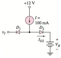
Figure P2.60
Expert Solution & Answer
Want to see the full answer?
Check out a sample textbook solution
Students have asked these similar questions
For the circuit shown in Figure 2-a, plot the output voltage across the resistance R, using the diode characteristic presented in Figure 2-b. Assume the input AC voltage supply given by
Vs = 1. sin(2pifot). Where fo = 100 Hz.
In addition, could you suggest a method on how to keep the output voltage more constant.
Q2
(b) Multiple diodes circuit is given in Figure
(i) Identify the condition for Si and Ge diodes.
(ii) Determine the current flowing into Si and Ge diodes.
(iii) Calculate the output voltage, Vo
accepting that D1 and D2 diodes have the same properties in the circuit given in the figurea) output voltage, b) current flowing through the resistor,c) current flowing from diodes calculate.
Chapter 2 Solutions
Microelectronics: Circuit Analysis and Design
Ch. 2 - Repeat Example 2.1 if the input voltage is...Ch. 2 - Consider the bridge circuit shown in Figure 2.6(a)...Ch. 2 - Assume the input signal to a rectifier circuit has...Ch. 2 - The input voltage to the halfwave rectifier in...Ch. 2 - Consider the circuit in Figure 2.4. The input...Ch. 2 - The circuit in Figure 2.5(a) is used to rectify a...Ch. 2 - The secondary transformer voltage of the rectifier...Ch. 2 - Determine the fraction (percent) of the cycle that...Ch. 2 - The Zener diode regulator circuit shown in Figure...Ch. 2 - Repeat Example 2.6 for rz=4 . Assume all other...
Ch. 2 - Consider the circuit shown in Figure 2.19. Let...Ch. 2 - Suppose the currentlimiting resistor in Example...Ch. 2 - Suppose the power supply voltage in the circuit...Ch. 2 - Design a parallelbased clipper that will yield the...Ch. 2 - Sketch the steadystate output voltage for the...Ch. 2 - Consider the circuit in Figure 2.23(a). Let R1=5k...Ch. 2 - Determine the steadystate output voltage O for the...Ch. 2 - Design a parallelbased clipper circuit that will...Ch. 2 - Consider the circuit shown in Figure 2.38, in...Ch. 2 - Consider the circuit shown in Figure 2.39. The...Ch. 2 - Repeat Example 2.11 for the case when R1=8k ,...Ch. 2 - The cutin voltage of each diode in the circuit...Ch. 2 - Prob. 2.12TYUCh. 2 - Consider the OR logic circuit shown in Figure...Ch. 2 - Consider the AND logic circuit shown in Figure...Ch. 2 - (a) Photons with an energy of hv=2eV are incident...Ch. 2 - Determine the value of resistance R required to...Ch. 2 - What characteristic of a diode is used in the...Ch. 2 - Prob. 2RQCh. 2 - Describe a simple fullwave diode rectifier circuit...Ch. 2 - Prob. 4RQCh. 2 - Prob. 5RQCh. 2 - Describe a simple Zener diode voltage reference...Ch. 2 - What effect does the Zener diode resistance have...Ch. 2 - What are the general characteristics of diode...Ch. 2 - Describe a simple diode clipper circuit that...Ch. 2 - Prob. 10RQCh. 2 - What one circuit element, besides a diode, is...Ch. 2 - Prob. 12RQCh. 2 - Describe a diode OR logic circuit. Compare a logic...Ch. 2 - Describe a diode AND logic circuit. Compare a...Ch. 2 - Describe a simple circuit that can be used to turn...Ch. 2 - Consider the circuit shown in Figure P2.1. Let...Ch. 2 - For the circuit shown in Figure P2.1, show that...Ch. 2 - A halfwave rectifier such as shown in Figure...Ch. 2 - Consider the battery charging circuit shown in...Ch. 2 - Figure P2.5 shows a simple fullwave battery...Ch. 2 - The fullwave rectifier circuit shown in Figure...Ch. 2 - The input signal voltage to the fullwave rectifier...Ch. 2 - The output resistance of the fullwave rectifier in...Ch. 2 - Repeat Problem 2.8 for the halfwave rectifier in...Ch. 2 - Consider the halfwave rectifier circuit shown in...Ch. 2 - The parameters of the halfwave rectifier circuit...Ch. 2 - The fullwave rectifier circuit shown in Figure...Ch. 2 - Consider the fullwave rectifier circuit in Figure...Ch. 2 - The circuit in Figure P2.14 is a complementary...Ch. 2 - Prob. 2.15PCh. 2 - A fullwave rectifier is to be designed using the...Ch. 2 - Prob. 2.17PCh. 2 - (a) Sketch o versus time for the circuit in Figure...Ch. 2 - Consider the circuit shown in Figure P2.19. The...Ch. 2 - Consider the Zener diode circuit shown in Figure...Ch. 2 - Consider the Zener diode circuit shown in Figure...Ch. 2 - In the voltage regulator circuit in Figure P2.21,...Ch. 2 - A Zener diode is connected in a voltage regulator...Ch. 2 - Consider the Zener diode circuit in Figure 2.19 in...Ch. 2 - Design a voltage regulator circuit such as shown...Ch. 2 - The percent regulation of the Zener diode...Ch. 2 - A voltage regulator is to have a nominal output...Ch. 2 - Consider the circuit in Figure P2.28. Let V=0 ....Ch. 2 - The secondary voltage in the circuit in Figure...Ch. 2 - The parameters in the circuit shown in Figure...Ch. 2 - Consider the circuit in Figure P2.31. Let V=0 (a)...Ch. 2 - Prob. 2.32PCh. 2 - Each diode cutin voltage is 0.7 V for the circuits...Ch. 2 - The diode in the circuit of Figure P2.34(a) has...Ch. 2 - Consider the circuits shown in Figure P2.35. Each...Ch. 2 - Plot O for each circuit in Figure P2.36 for the...Ch. 2 - Consider the parallel clipper circuit in Figure...Ch. 2 - A car’s radio may be subjected to voltage spikes...Ch. 2 - Sketch the steadystate output voltage O versus...Ch. 2 - Prob. D2.40PCh. 2 - Design a diode clamper to generate a steadystate...Ch. 2 - For the circuit in Figure P2.39(b), let V=0 and...Ch. 2 - Repeat Problem 2.42 for the circuit in Figure...Ch. 2 - The diodes in the circuit in Figure P2.44 have...Ch. 2 - In the circuit in Figure P2.45 the diodes have the...Ch. 2 - The diodes in the circuit in Figure P2.46 have the...Ch. 2 - Consider the circuit shown in Figure P2.47. Assume...Ch. 2 - The diode cutin voltage for each diode in the...Ch. 2 - Consider the circuit in Figure P2.49. Each diode...Ch. 2 - Assume V=0.7V for each diode in the circuit in...Ch. 2 - The cutin voltage of each diode in the circuit...Ch. 2 - Let V=0.7V for each diode in the circuit in Figure...Ch. 2 - For the circuit shown in Figure P2.54, let V=0.7V...Ch. 2 - Assume each diode cutin voltage is V=0.7V for the...Ch. 2 - If V=0.7V for the diode in the circuit in Figure...Ch. 2 - Let V=0.7V for the diode in the circuit in Figure...Ch. 2 - Each diode cutin voltage in the circuit in Figure...Ch. 2 - Let V=0.7V for each diode in the circuit shown in...Ch. 2 - Consider the circuit in Figure P2.61. The output...Ch. 2 - Consider the circuit in Figure P2.62. The output...Ch. 2 - Prob. 2.63PCh. 2 - Consider the circuit shown in Figure P2.64. The...Ch. 2 - The lightemitting diode in the circuit shown in...Ch. 2 - The parameters of D1 and D2 in the circuit shown...Ch. 2 - If the resistor in Example 2.12 is R=2 and the...Ch. 2 - Consider the photodiode circuit shown in Figure...Ch. 2 - Consider the fullwave bridge rectifier circuit....Ch. 2 - Design a simple dc voltage source using a...Ch. 2 - A clipper is to be designed such that O=2.5V for...Ch. 2 - Design a circuit to provide the voltage transfer...
Knowledge Booster


Learn more about
Need a deep-dive on the concept behind this application? Look no further. Learn more about this topic, electrical-engineering and related others by exploring similar questions and additional content below.Similar questions
- In the circuit, diode D1 has n = 1.4 and has an operating point I D = 1mA at V D =0.7 V and is at room temperature. Diode D2 has an area that is 20 times larger than D1 but isotherwise the same. a) What is the current through diode D1?b) What is the value of the saturation current, Is for diode D2?c) What is the voltage Vx ? d) Determine the value of R to make Vo = -0.2Varrow_forwardHow are diodes tested for functionality? Write the necessary devices/materials needed to do the test and discuss thoroughly the procedure.arrow_forwardCalculate the V0 voltage and the ID1 current in the circuit given with figure 2, If R1=10kohm, R2=5kohm and forward diode voltage is 0.7V ..arrow_forward
- ⦁ Consider the below zener diode circuit and find the values of , , , . Use the constant voltage drop model which is shown is Figure 2. Show your solution steps clearly and explain them. The answers without solution steps will not be graded. Also, state your results in the sections below the circuits. ( = 0.1 )arrow_forwardIn one graph, sketch the I-V curve for the forward bias. Forward Bias of PN Junction Diode:1. The Cut in Voltage or Knee Voltage of 1N4148 is _____________Volts.2. The Static Forward resistance of 1N4148 is __________________ .arrow_forwardCompare the application of zener diode and regular diode in a DC power supplysystem.(a) Describe their different function and operation in the DC supply system.(b) Can zener replace the function of the regular diode in the application describedin question 3(a)? Justify your answer.arrow_forward
- For the half-wave rectifier circuit shown, the diode is not ideal and is modeled as an ideal voltage source of value Vf= =0.65V in series with an ideal diode. Vin= 2sin(2π10t) and R= 470Ω. What is the magnitude of the diode current at time t=60mst=60ms? 2- At what time between 0and T/4 seconds is the magnitude of the diode current equal to 2.66mA? Tis the period of Vin Enter your answer in millisecondsarrow_forwardFor the following circuit; a)- Diodes' conduction-cut status ("On" or "Off") determine mathematically.? (For diodes voltage drop model will be used. For each diode Vd = 0.7 V). b)- Currents passing through all branches of the circuit calculate? c)- 10 kΩ resistor on the right of the circuit Calculate the power spent on it.arrow_forward1) Copy the diagram of a semiconductor junction diode. Show its p-type and n-type regions and the depletion region. (a) When the diode is forward biased:What happens to the barrier potential?What happens to the depletion region?Indicate on your diagram the directions in which the holes and electrons move.(b) When the diode is reverse biased, Why the diode becomes less conductive?arrow_forward
- Q1 (a) For the given circuit in Figure Q1.1, (i) Describe the diode representation as a switch (ii) Identify the condition of the diode and its equivalent circuit. (iii) Calculate ID, VR1, VR2 and Vo with the diode represent as a switch. (iv) Perform the same calculation as (ii) for GaAs diode.arrow_forwarda. Using standard resistor values, what value of R1 is needed to achieve 1.18V ±0.01V at Vout? b. Using the R1 value chosen in (a) part, what happens to the voltage Vout when a load resistance of 10K is added (between Vout and ground). c. What is the minimum value of load resistance required for correct operation Zener diode is used in place of si diode. Or you can assume zener current according to requirement Answer it i will ratearrow_forwardIn the circuit shown in Figure 2–52 (p. 97), the Zener diode has a reverse breakdown voltage of 12V. RS = 50 Ohms, VS = 20V, and RL can vary from 100 Ohms to 200 Ohms. Assuming that the Zener diode remains in breakdown, find: (a) the minimum and maximum current in the Zener diode; (b) the minimum and maximum power dissipated in the diode; and (c) the minimum rated power dissipation that RS should have.arrow_forward
arrow_back_ios
SEE MORE QUESTIONS
arrow_forward_ios
Recommended textbooks for you

Diodes Explained - The basics how diodes work working principle pn junction; Author: The Engineering Mindset;https://www.youtube.com/watch?v=Fwj_d3uO5g8;License: Standard Youtube License