
Concept explainers
Videos
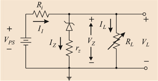
Consider the Zener diode circuit in Figure 2.19 in the text. Assume parameter values of
(a)
The value of
Answer to Problem 2.24P
Explanation of Solution
Given:
The given circuit is
Calculation:
For
Apply KVL in loop 1,
Therefore, the load voltage will be
Thus, the power dissipated will be
(b)
The value of
Answer to Problem 2.24P
Explanation of Solution
Given:
The given circuit is

Calculation:
For
Apply KCL at the center node,
As
By substituting the value of
Hence, the load voltage will be
Thus, the load current can be calculated as
Thus, the power dissipated will be equal to
(c)
The value of
Answer to Problem 2.24P
Explanation of Solution
Given:
The given circuit is

Calculation:
For
Apply KVL in loop 1,
Therefore, the load voltage will be
Thus, the power dissipated will be
(d)
The value of
Answer to Problem 2.24P
Explanation of Solution
Given:
The given circuit is

Calculation:
For
Apply KCL at the center node,
As
By substituting the value of
Hence, the load voltage will be
Thus, the load current can be calculated as
Thus, the power dissipated will be equal to
Want to see more full solutions like this?
Chapter 2 Solutions
Microelectronics: Circuit Analysis and Design


- For the half-wave rectifier circuit shown, the diode is not ideal and is modeled as an ideal voltage source of value Vf= =0.65V in series with an ideal diode. Vin= 2sin(2π10t) and R= 470Ω. What is the magnitude of the diode current at time t=60mst=60ms? 2- At what time between 0and T/4 seconds is the magnitude of the diode current equal to 2.66mA? Tis the period of Vin Enter your answer in millisecondsarrow_forward2.13 Two diodes are connected in series as shown in Figure 2.11a to share a total de reverse volt age of VD=5 KV. The reverse leakage currents of two diode I=25 mA, 1,2 = 30 mA. (a) Find the diode voltage if the voltage sharing resistances R₁ and R₂ are equal R₁ = R₂ = 200 KN. (b) Find the voltage sharing resistance R₁ and R₂ if the diode voltage are equal Vd1= Vd2= Vd/2arrow_forwardCan you answer the question by explaining step by step and explaining why you used that formula or calculations in details please. Thanks a lot. 2) Consider a two terminal semiconductor diode a) Calculate the thermal voltage of a diode at room temperature about 27oC b) Calculate diode dynamic resistance in case of 13 mA diode current. (Boltzman’s constant is 1.38x10⁻²³ J/K, and magnitude of electron charge is 1,6X10⁻¹⁹ C)arrow_forward
- please answer (vii) that is the graph Calculate the following about the circuit in Figure 2.1 (If silicon diodes are employed in the rectification); i. the peak value of the output voltage considering the drop across each diode, Vpk. ii. the average voltage, Vdc. iii. The current through the load resistor, IL. iv. The current diode, Id. v. The frequency of the output signal, Fout. vi. Calculate the efficiency of the full wave rectifier expressed in percentage. vii. Sketch a graph of the input and output voltage against time.arrow_forwardP-types silicon sample is 0.2cm long and has a rectangular cross section 0.03cm² .The accepter concentration is 5x10^18 holes/cm³. The mobility is 100. A current of 10µA exists in the bar. Determine the electron and hole concentrations, the conductivity, current density,velocity of electrons, the voltage across the bar and reristance.ni=10^10.arrow_forwardApply each of diodeapproximations and determine:a. Current through D1b. Voltage across D2c. Voltage across R3 GIVEN: R1 = 2 kΩ, R2 = 1.2 kΩ, R3 = 6.8 kΩ E= 10 V D1: Si, rB = 2 Ω, rR = 220 kΩ D2: Si, rB = 5 Ω, rR = 560 kΩ DETERMING FIRST IF IT IS A FORWARD BIASED OR REVERSED BIASED THEN, SOLVE IN FIRST APPROXIMATION, SECOND APPROXIMATION AND THIRD APPROXIMATION SHOW THE CIRCUIT DIAGRAM IN EACH APPROXIMATIONarrow_forward
- DEVELOP AND JUSTIFY YOUR RESPONSE. Determine the total current when BT1 = 15.9 V, BT2 = 7.5 V, the Resistance R1 = 1.1 kΩ and the Resistance R2 = 4.4 kΩ, Consider voltage drop of the diodes of Si = 0.7V A. -2.55 mA. B. 1,40 mA. C. 4.25 mA. D. -1.53 mA.arrow_forwardCalculate the V0 voltage and the ID1 current in the circuit given with figure 2, If R1=10kohm, R2=5kohm and forward diode voltage is 0.7V ..arrow_forwardIn the given system; Va, Vb, Vc effective value is 220V, Ly=300 mH and Ry=22 Ohms.It was observed that the yuk current is continuous when the tristorier is triggered for alpha=65 degrees; and D1the average value of the diode current was calculated as ID1 avg = 1.703A.Accordingly, calculate the average value of the current flowing through T3. IT3_ avg=?arrow_forward
- 1) Copy the diagram of a semiconductor junction diode. Show its p-type and n-type regions and the depletion region. (a) When the diode is forward biased:What happens to the barrier potential?What happens to the depletion region?Indicate on your diagram the directions in which the holes and electrons move.(b) When the diode is reverse biased, Why the diode becomes less conductive?arrow_forwardConsider the diodes D1, D2, and D3 type as Silicon, Germanium, and GaAs respectively. Calculate for the current in each diode, and the voltage across R1arrow_forwardFill in the blanks with the words belowcheck valve, conductance, convert, crystalline, impurities, infinite, galena, p–n junction, rectifying,resistance, selenium, semiconductor, switching circuits, tailored, temperature, threshold, two-terminal,unidirectionalA diode is a 1 ………………… electronic component that conducts current primarily in one direction(asymmetric 2 ………………..); it has low (ideally zero) 3 ……………… in one direction, and high (ideally4 ………………..) resistance in the other. A 5 ………….. diode, the most common type today, is a 6……….. piece of semiconductor material with a 7 ………………. connected to two electrical terminals. Avacuum tube diode has two electrodes, a plate (anode) and a heated cathode. Semiconductor diodes were thefirst semiconductor electronic devices. The discovery of crystals' 8 ……………… abilities was made byGerman physicist Ferdinand Braun in 1874. The first semiconductor diodes, developed around 1906, weremade of mineral crystals such as 9 ……………….. . Today, most…arrow_forward
