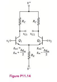
Consider the differential amplifier shown in Figure P11.14 with mismatched transistors. The mismatched transistors result in mismatched transconductances as shown. The circuit and transistor parameters are V + = + 10 V , V − = − 10 V , R C = 50 k Ω , R E = 75 k Ω , β = 120 V B E ( on ) = 0.7 V , and V A = ∞ . Determine A d , A c m , and CMRRlag for Δ g m / g m = 0.01 and for v O = v C 1 − v C 2 . Assume v 1 = v 2 = 0 in the quiescent condition.
Consider the differential amplifier shown in Figure P11.14 with mismatched transistors. The mismatched transistors result in mismatched transconductances as shown. The circuit and transistor parameters are V + = + 10 V , V − = − 10 V , R C = 50 k Ω , R E = 75 k Ω , β = 120 V B E ( on ) = 0.7 V , and V A = ∞ . Determine A d , A c m , and CMRRlag for Δ g m / g m = 0.01 and for v O = v C 1 − v C 2 . Assume v 1 = v 2 = 0 in the quiescent condition.
Solution Summary: The author calculates the differential-mode gain, common-mod gain and common mode rejection ratios for the given circuit.
Consider the differential amplifier shown in Figure P11.14 with mismatched transistors. The mismatched transistors result in mismatched transconductances as shown. The circuit and transistor parameters are
V
+
=
+
10
V
,
V
−
=
−
10
V
,
R
C
=
50
k
Ω
,
R
E
=
75
k
Ω
,
β
=
120
V
B
E
(
on
)
=
0.7
V
,
and
V
A
=
∞
.
Determine
A
d
,
A
c
m
,
and CMRRlag for
Δ
g
m
/
g
m
=
0.01
and for
v
O
=
v
C
1
−
v
C
2
.
Assume
v
1
=
v
2
=
0
in the quiescent condition.
Consider the common-source amplifier shown in Figure P11.50. The NMOS transistor has KP=50 μA/V2, L=5 μm, W=500 μm, Vto=1 V and rd=∞.a. Determine the values of IDQ, VDSQ and gm. b. Compute the voltage gain, input resistance, and output resistance, assuming that the coupling capacitors are short circuits for the ac signal.
Repeat Problem P11.50 for an NMOS transistor having KP=50 μA/V2, W=600 μm, L=20 μm, Vto=2 V and rd=∞. Compare the gain with that attained in Problem P11.50.
The transistor parameters for the differential amplifier shown in Figure P11.32 are VT N = 0.5 V, k n = 80 µA/V2, W/L = 4, and λ = 0. (a) Find RD and IQ such that ID1 = ID2 = 80 µA and vO2 = 2 V when v1 = v2 = 0. (b) Draw the dc load line, and plot the Q-point for M2. (c) What is the maximum common-mode input voltage?
Figure p11.32
For the differential amplifier circuit below, all transistors are identical ( ?≠0 )
a) Draw the single-sided differential mode equivalent circuit, showing all details and labels Explain how you obtained this equivalent circuit
Need a deep-dive on the concept behind this application? Look no further. Learn more about this topic, electrical-engineering and related others by exploring similar questions and additional content below.


 Power System Analysis and Design (MindTap Course ...Electrical EngineeringISBN:9781305632134Author:J. Duncan Glover, Thomas Overbye, Mulukutla S. SarmaPublisher:Cengage Learning