
Concept explainers
(a)
To show: The expression for the value of the current
(a)
Explanation of Solution
Given:
The given circuit is shown in Figure 1
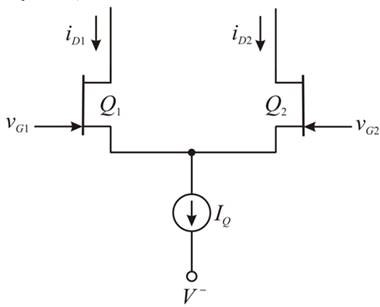
Figure 1
Calculation:
The expression for the current
The expression for the current
Both the JFET are matching so,
The expression to determine the value of the differential mode voltage is given by,
So the difference of current is,
The value of the sum of the drain current is given by,
So,
Square both the sides of the above equation.
Again square both the sides of the equation.
Solve further as,
The expression for the current
Conclusion:
Therefore, the expression for current ratios are
(b)
To show: The base current is switched to other transistor when
(b)
Explanation of Solution
Given:
The given circuit is shown in Figure 1
Figure 1
Calculation:
The diagram for the normalized dc transfer characteristics of MOSFET differential amplifier as a function of differential input voltage is shown in Figure 2
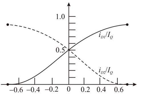
Figure 2
The expression to derive the expression for the differential input voltage is given by,
Therefore, the expression for the normalized differential voltage is given by,
Conclusion:
Therefore, the required expression is
(c)
To show: The expression for the maximum forward transconductance is
(c)
Explanation of Solution
Calculation:
The expression for the current
Differentiate both the sides of the equation.
Conclusion:
Therefore, the expression for conductance is
Want to see more full solutions like this?
Chapter 11 Solutions
Microelectronics: Circuit Analysis and Design


- Determine the amount of distributed generation active power that can besafely fed to a 400V line with Z= 0.3 + j0.9 Ω, if the maximum allowablevoltage rise is 4V and reactive power is negligible.arrow_forward2)A factory consumes a total power of 2000kW, with a power factor of 0.6 of a transformer whose primary voltage is 6kV. A synchronous capacitor is purchased to improve overall fp. Assuming that the losses in the synchronous capacitor are of 25kW, calculate:a) The original reactive power of the inductive loadb) The correction reactive power necessary to raise the power factorc) The nominal kVA power of the synchronous capacitor and its pf.arrow_forwardPOWER SİSTEMS high voltage technique it is possible to measure pulsed (AND ANSWER THE SAME QUESTION FOR AC AND DC ) high voltages with the help of two spheres of equal radius placed on the same axis. In which case the approximate impulse,AC AND DC voltage value that can be measured with such a system with diameters of 500 mm and known spacing between them is 2.5 cm, is given correctly. (Ambient conditions are neglected and take Ed = 30 kV / cm2 k = 0.9) a) 68,65114 kV b) 81.30081 kv c) 97,08737 kv d) 65,35947 kv e) 57.48835 kv f) 46.21612 kv PLEASE ANSWER THE SAME QUESTION FOR DC HİGH VOLTAGE AND AC HİGH VOLTAGE WHAT THE DIFFERENCE BETWEEN THEMarrow_forward
- A 120Hp engine. of 380VAC,60Hz, f.p =.0.65(-), n = 69% is connected in parallel with an 80Kw industrial oven. more 50kw luminaires, f.p =0.4(-). The company orders the power factor to be corrected to 0.9. a) Deduct what is necessary for this purpose.arrow_forwarda coil of unknown resistance and a reactance of j8 Ohms is in parallel with a pure capacitor of -j16 Ohms reactance.Determine all possible values of coil resistance if the total impedance is 16 Ohms at a power factor of 0.96.\ Answer/s: 6 ohms (if lagging pf) 10.6667 Ohms (if leading pf)arrow_forwardA HV transmission line having receiving end load is 300MVA, 50 Hz line from poin A to point B. Resistance 0.13 ohm/KM , for 160 KM Inductance XL= 0.4 ohm per kilometer Parallel admittance j318 × 10-6 Power Factor 0.8770, 0.8477 lagging, unity and 0.8770, 0.8477 leading Assume desired voltage at the receiving end of the transmission line is not less than 380kV., if the line is supplying rated voltage and apparent power at various power factors given Estimate : a. Sending end voltages b. Voltage regulation c. Efficiency of the transmission line d. Give a technical explanations on the results obtainedarrow_forward
- Determine the output voltage for the circuit of Fig. 11.52arrow_forward. At a 12.47 kV (line to line) distribution system the communication interference (CI) was observed due to 5% of 5th harmonic currents generated by a 3000 kVA arc furnace. In order to avoid CI it is required to convert an existing 600 kVAr capacitor to 5th harmonic filter considering the total kVAr should not exceed 135%. Calculate the following: (i) Capacitor reactance (ii) Reactance of the series reactor (iii) Fundamental frequency current (iv) 5th harmonic frequency current (v) Tuned frequency voltage (vi) Total rms current (vii) Fundamental frequency voltage (viii) Voltage (rms) across the capacitor bank (ix) Check whether the filter kVAr rating is within limit? (x) Comment how the existing capacitor bank is converted to filterarrow_forwardfive infinite-impedance volunteers,calibrated to read rms values,are connected as shown below. let R= 200, L=0.400H,C=6.0 Mf, and V=30.0 v. what's the reading of the voltmeter's V1,V2,V3,V4 and V5 if W= 200 rad/sarrow_forward
- A 12-stage impulse voltage generator has a capacitor C. The wave front resistance equal to 0.6kΩ and wave tail resistance 7019Ω. If the wave front and wave tail times of the impulse wave are 2 μs and 0.06 ms respectively. Calculate (i) the capacitance of each capacitor in the generator and (ii) the capacitance of the load capacitor (C2)?arrow_forwarda. A single-phase semi-converter supplies an inductive load having an impedance of 3k. Assume that the output current is constant and is equal to Id. If the supply voltage is 220V and the firing angle is maintained at /2, calculate (i) Average output voltage, (ii) Supply RMS current, (iii) Supply fundamental RMS current.arrow_forwardRA = 17.32 ohms, LA = 0.0318 H, ZB = 5ohms, XB = j4 ohms in series connected A and B coils. When a voltage of U = 240 V, 50 Hz is applied to this circuit; a) How many Amps will the Circuit Current be? b) Active and reactive powers of A and B coils Calculate.arrow_forward
 Introductory Circuit Analysis (13th Edition)Electrical EngineeringISBN:9780133923605Author:Robert L. BoylestadPublisher:PEARSON
 Delmar's Standard Textbook Of ElectricityElectrical EngineeringISBN:9781337900348Author:Stephen L. HermanPublisher:Cengage Learning
 Programmable Logic ControllersElectrical EngineeringISBN:9780073373843Author:Frank D. PetruzellaPublisher:McGraw-Hill Education
 Fundamentals of Electric CircuitsElectrical EngineeringISBN:9780078028229Author:Charles K Alexander, Matthew SadikuPublisher:McGraw-Hill Education
 Electric Circuits. (11th Edition)Electrical EngineeringISBN:9780134746968Author:James W. Nilsson, Susan RiedelPublisher:PEARSON
 Engineering ElectromagneticsElectrical EngineeringISBN:9780078028151Author:Hayt, William H. (william Hart), Jr, BUCK, John A.Publisher:Mcgraw-hill Education,